- 您現(xiàn)在的位置:買(mǎi)賣(mài)IC網(wǎng) > PDF目錄362579 > E28F016SA-070 (INTEL CORP) 28F016SA 16-MBIT (1 MBIT X 16, 2 MBIT X 8)FlashFile MEMORY PDF資料下載
參數(shù)資料
| 型號(hào): | E28F016SA-070 |
| 廠商: | INTEL CORP |
| 元件分類(lèi): | PROM |
| 英文描述: | 28F016SA 16-MBIT (1 MBIT X 16, 2 MBIT X 8)FlashFile MEMORY |
| 中文描述: | 1M X 16 FLASH 12V PROM, 70 ns, PDSO56 |
| 封裝: | 20 X 14 MM, 1.20 MM HEIGHT, TSOP1-56 |
| 文件頁(yè)數(shù): | 7/37頁(yè) |
| 文件大?。?/td> | 611K |
| 代理商: | E28F016SA-070 |
第1頁(yè)第2頁(yè)第3頁(yè)第4頁(yè)第5頁(yè)第6頁(yè)當(dāng)前第7頁(yè)第8頁(yè)第9頁(yè)第10頁(yè)第11頁(yè)第12頁(yè)第13頁(yè)第14頁(yè)第15頁(yè)第16頁(yè)第17頁(yè)第18頁(yè)第19頁(yè)第20頁(yè)第21頁(yè)第22頁(yè)第23頁(yè)第24頁(yè)第25頁(yè)第26頁(yè)第27頁(yè)第28頁(yè)第29頁(yè)第30頁(yè)第31頁(yè)第32頁(yè)第33頁(yè)第34頁(yè)第35頁(yè)第36頁(yè)第37頁(yè)
E
BYTE-WIDE SMART 5 FlashFile MEMORY FAMILY
7
PRODUCT PREVIEW
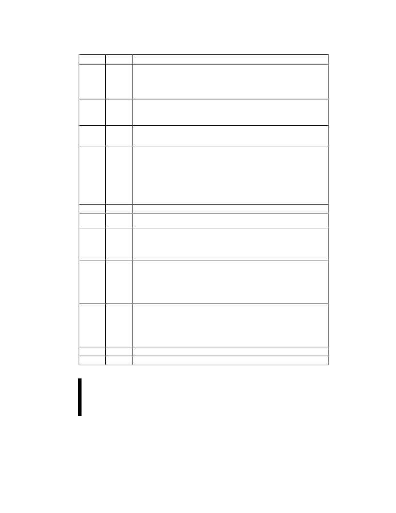
Table 1. Pin Descriptions
Sym
Type
Name and Function
A
0
–A
20
INPUT
ADDRESS INPUTS:
Inputs for addresses during read and write operations.
Addresses are internally latched during a write cycle.
4Mbit
→
A
0
–A
18
8Mbit
→
A
0
–A
19
16Mbit
→
A
0
–A
20
DATA INPUT/OUTPUTS:
Inputs data and commands during CUI write cycles;
outputs data during memory array, status register, and identifier code read cycles.
Data pins float to high-impedance when the chip is deselected or outputs are
disabled. Data is internally latched during a write cycle.
DQ
0
–DQ
7
INPUT/
OUTPUT
CE#
INPUT
CHIP ENABLE:
Activates the device’s control logic, input buffers, decoders, and
sense amplifiers. CE#-high deselects the device and reduces power consumption to
standby levels.
RP#
INPUT
RESET/DEEP POWER-DOWN:
When driven low, RP# inhibits write operations
which provides data protection during power transitions, puts the device in deep
power-down mode, and resets internal automation. RP#-high enables normal
operation. Exit from deep power-down sets the device to read array mode.
RP# at V
HH
enables setting of the master lock-bit and enables configuration of block
lock-bits when the master lock-bit is set. RP# = V
HH
overrides block lock-bits,
thereby enabling block erase and program operations to locked memory blocks.
Block erase, program, or lock-bit configuration with V
IH
< RP# < V
HH
produce
spurious results and should not be attempted.
OE#
INPUT
OUTPUT ENABLE:
Gates the device’s outputs during a read cycle.
WE#
INPUT
WRITE ENABLE:
Controls writes to the CUI and array blocks. Addresses and data
are latched on the rising edge of the WE# pulse.
RY/BY#
OUTPUT
READY/BUSY#:
Indicates the status of the internal WSM. When low, the WSM is
performing an internal operation (block erase, program, or lock-bit configuration).
RY/BY#-high indicates that the WSM is ready for new commands, block erase or
program is suspended, or the device is in deep power-down mode. RY/BY# is
always active.
V
PP
SUPPLY
BLOCK ERASE, PROGRAM, LOCK-BIT CONFIGURATION POWER SUPPLY:
For erasing array blocks, programming data, or configuring lock-bits.
Smart 5 Flash
→
5V and 12V V
PP
With V
PP
≤
V
PPLK
, memory contents cannot be altered. Block erase, program, and
lock-bit configuration with an invalid V
PP
(see DC Characteristics) produce spurious
results and should not be attempted.
V
CC
SUPPLY
DEVICE POWER SUPPLY:
Internal detection automatically configures the device
for optimized read performance. Do not float any power pins.
Smart 5 Flash
→
5V V
CC
With V
CC
≤
V
LKO
, all write attempts to the flash memory are inhibited. Device
operations at invalid V
CC
voltages (see DC Characteristics) produce spurious
results and should not be attempted.
GND
SUPPLY
GROUND:
Do not float any ground pins.
NC
NO CONNECT:
Lead is not internally connected; it may be driven or floated.
相關(guān)PDF資料 |
PDF描述 |
|---|---|
| E28F016SA-080 | 28F016SA 16-MBIT (1 MBIT X 16, 2 MBIT X 8)FlashFile MEMORY |
| E28F016SA-100 | 28F016SA 16-MBIT (1 MBIT X 16, 2 MBIT X 8)FlashFile MEMORY |
| E28F016SA-120 | 28F016SA 16-MBIT (1 MBIT X 16, 2 MBIT X 8)FlashFile MEMORY |
| E28F016SA-150 | 28F016SA 16-MBIT (1 MBIT X 16, 2 MBIT X 8)FlashFile MEMORY |
| E28F016SC-120 | BYTE-WIDE SmartVoltage FlashFile MEMORY FAMILY 4, 8, AND 16 MBIT |
相關(guān)代理商/技術(shù)參數(shù) |
參數(shù)描述 |
|---|---|
| E28F016SA-080 | 制造商:INTEL 制造商全稱(chēng):Intel Corporation 功能描述:28F016SA 16-MBIT (1 MBIT X 16, 2 MBIT X 8)FlashFile MEMORY |
| E28F016SA-100 | 制造商:INTELC 功能描述: |
| E28F016SA-120 | 制造商:INTEL 制造商全稱(chēng):Intel Corporation 功能描述:28F016SA 16-MBIT (1 MBIT X 16, 2 MBIT X 8)FlashFile MEMORY |
| E28F016SA-150 | 制造商:INTEL 制造商全稱(chēng):Intel Corporation 功能描述:28F016SA 16-MBIT (1 MBIT X 16, 2 MBIT X 8)FlashFile MEMORY |
| E28F016SA70 | 制造商:未知廠家 制造商全稱(chēng):未知廠家 功能描述:x8/x16 Flash EEPROM |
發(fā)布緊急采購(gòu),3分鐘左右您將得到回復(fù)。