- 您現(xiàn)在的位置:買賣IC網(wǎng) > PDF目錄376997 > DSM2180F3V15K6 (意法半導(dǎo)體) DSM (Digital Signal Processor System Memory) For Analog Devices ADSP-218X Family (5V Supply) PDF資料下載
參數(shù)資料
| 型號(hào): | DSM2180F3V15K6 |
| 廠商: | 意法半導(dǎo)體 |
| 元件分類: | 數(shù)字信號(hào)處理 |
| 英文描述: | DSM (Digital Signal Processor System Memory) For Analog Devices ADSP-218X Family (5V Supply) |
| 中文描述: | 帝斯曼(數(shù)字信號(hào)處理器系統(tǒng)內(nèi)存)模擬器件公司的ADSP - 218X系列(5V電源) |
| 文件頁(yè)數(shù): | 10/63頁(yè) |
| 文件大小: | 809K |
| 代理商: | DSM2180F3V15K6 |
第1頁(yè)第2頁(yè)第3頁(yè)第4頁(yè)第5頁(yè)第6頁(yè)第7頁(yè)第8頁(yè)第9頁(yè)當(dāng)前第10頁(yè)第11頁(yè)第12頁(yè)第13頁(yè)第14頁(yè)第15頁(yè)第16頁(yè)第17頁(yè)第18頁(yè)第19頁(yè)第20頁(yè)第21頁(yè)第22頁(yè)第23頁(yè)第24頁(yè)第25頁(yè)第26頁(yè)第27頁(yè)第28頁(yè)第29頁(yè)第30頁(yè)第31頁(yè)第32頁(yè)第33頁(yè)第34頁(yè)第35頁(yè)第36頁(yè)第37頁(yè)第38頁(yè)第39頁(yè)第40頁(yè)第41頁(yè)第42頁(yè)第43頁(yè)第44頁(yè)第45頁(yè)第46頁(yè)第47頁(yè)第48頁(yè)第49頁(yè)第50頁(yè)第51頁(yè)第52頁(yè)第53頁(yè)第54頁(yè)第55頁(yè)第56頁(yè)第57頁(yè)第58頁(yè)第59頁(yè)第60頁(yè)第61頁(yè)第62頁(yè)第63頁(yè)
DSM2180F3
10/63
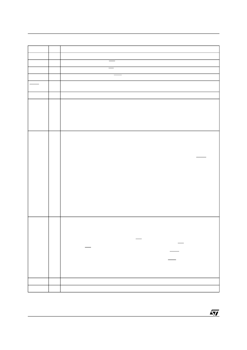
Table 3. Pin Description
Pin Name
Type
Description
ADIO0-15
In
Sixteen address inputs from the DSP
CNTL0
In
Active low write strobe input (WR) from the DSP
CNTL1
In
Active low read strobe input (RD) from the DSP.
CNTL2
In
Active low Byte Memory Select (BMS) signal from the DSP.
Reset
In
Active low reset input from system. Resets DSM I/O Ports, Page Register contents, and other
DSM configuration registers. Must be logic Low at Power-up.
PA0-7
I/O
Eight data bus signals connected to DSP pins D8 - D15.
PB0-7
I/O
Eight configurable Port B signals with the following functions:
1. MCU I/O – DSP may write or read pins directly at runtime with csiop registers.
2. CPLD Output Macrocell (McellAB0-7 or McellBC0-7) outputs.
3. Inputs to the PLDs (Input Macrocells).
Note: Each of the four Port B signals PB0-PB3 may be configured at run-time as either standard
CMOS or for high slew rate. Each of the four Port B signals PB3-PB7 may be configured at
run-time as either standard CMOS or Open Drain Outputs.
PC0-7
I/O
Eight configurable Port C signals with the following functions:
1. MCU I/O – DSP may write or read pins directly at runtime with csiop registers.
2. CPLD Output Macrocell (McellBC0-7) output.
3. Input to the PLDs (Input Macrocells).
4. Pins PC0, PC1, PC5, and PC6 can optionally form the JTAG IEEE-1149.1 ISP serial
interface as signals TMS, TCK, TDI, and TDO respectively.
5. Pins PC3 and PC4 can optionally form the enhanced JTAG signals TSTAT and TERR
respectively. Reduces ISP programming time by up to 30% when used in addition to the
standard four JTAG signals: TDI, TDO, TMS, TCK.
6. Pin PC3 can optionally be configured as the Ready/Busy output to indicate Flash memory
programming status during parallel programming. May be polled by DSP or used as DSP
interrupt to indicate when Flash memory byte programming or erase operations are
complete.
Note 1: Port C pin PC2 input (or any PLD input pin) can be connected to DSP D18 output which
functions as DSP address A16 in DSP Full Memory Mode. See Figure 6.
Note 2: Port C pin PC7 input (or any PLD input pin) can be connected to DSP D19 output which
functions as DSP address A17 in DSP Full Memory Mode. See Figure 6.
Note 3: When used as general I/O, each of the eight Port C signals may be configured at run-time
as either standard CMOS or Open Drain Outputs.
Note 4: The JTAG ISP pins may be multiplexed with other I/O functions.
PD0-2
I/O
Three configurable Port D signals with the following functions:
1. MCU I/O – DSP may write or read pins directly at runtime with csiop registers.
2. Input to the PLDs (no associated Input Macrocells, routes directly into PLDs).
3. CPLD output (External Chip Select). Does not consume Output Macrocells.
4. Pin PD1 can optionally be configured as CLKIN, a common clock input to PLD.
5. Pin PD2 can optionally be configured as CSI, an active low Chip Select Input to select Flash
memory. Flash memory is disabled to conserve more power when CSI is logic high. Can
connect CSI to ADSP-218X PWDACK output signal.
Note 1: It is recommended to connect Port D pin PD0 input to DSP IOMS output which is the
active low I/O Memory Select strobe. See Figure 6.
Note 2: It is recommended to connect Port D pin PD1 input to DSP DMS output which is the active
low Data Memory Select strobe. See Figure 6.
Note 3: It is recommended to connect Port D pin PD2 input to DSP PWDACK output if the DSP
Power Down mode is used. See Figure 6.
V
CC
Supply Voltage
GND
Ground pins
相關(guān)PDF資料 |
PDF描述 |
|---|---|
| DSM2180F3V15T6 | DSM (Digital Signal Processor System Memory) For Analog Devices ADSP-218X Family (5V Supply) |
| DSM2180F3V90K6 | DSM (Digital Signal Processor System Memory) For Analog Devices ADSP-218X Family (5V Supply) |
| DSM2180F3V90T6 | DSM (Digital Signal Processor System Memory) For Analog Devices ADSP-218X Family (5V Supply) |
| DSM2190F4 | 16-bit fixed point DSP with Flash |
| DSM2190F4V | 16-bit fixed point DSP with Flash |
相關(guān)代理商/技術(shù)參數(shù) |
參數(shù)描述 |
|---|---|
| DSM2180F3V-15K6 | 功能描述:SPLD - 簡(jiǎn)單可編程邏輯器件 5.0V 8M 150ns RoHS:否 制造商:Texas Instruments 邏輯系列:TICPAL22V10Z 大電池?cái)?shù)量:10 最大工作頻率:66 MHz 延遲時(shí)間:25 ns 工作電源電壓:4.75 V to 5.25 V 電源電流:100 uA 最大工作溫度:+ 75 C 最小工作溫度:0 C 安裝風(fēng)格:Through Hole 封裝 / 箱體:DIP-24 |
| DSM2180F3V15T6 | 制造商:STMICROELECTRONICS 制造商全稱:STMicroelectronics 功能描述:DSM (Digital Signal Processor System Memory) For Analog Devices ADSP-218X Family (3.3V Supply) |
| DSM2180F3V-15T6 | 功能描述:SPLD - 簡(jiǎn)單可編程邏輯器件 5.0V 8M 150ns RoHS:否 制造商:Texas Instruments 邏輯系列:TICPAL22V10Z 大電池?cái)?shù)量:10 最大工作頻率:66 MHz 延遲時(shí)間:25 ns 工作電源電壓:4.75 V to 5.25 V 電源電流:100 uA 最大工作溫度:+ 75 C 最小工作溫度:0 C 安裝風(fēng)格:Through Hole 封裝 / 箱體:DIP-24 |
| DSM2180F3V90K6 | 制造商:STMICROELECTRONICS 制造商全稱:STMicroelectronics 功能描述:DSM (Digital Signal Processor System Memory) For Analog Devices ADSP-218X Family (3.3V Supply) |
| DSM2180F3V-90K6 | 制造商:未知廠家 制造商全稱:未知廠家 功能描述:ASIC |
發(fā)布緊急采購(gòu),3分鐘左右您將得到回復(fù)。