- 您現(xiàn)在的位置:買賣IC網(wǎng) > PDF目錄223667 > DS75361 (National Semiconductor Corporation) Dual TTL-to-MOS Driver PDF資料下載
參數(shù)資料
| 型號: | DS75361 |
| 廠商: | National Semiconductor Corporation |
| 英文描述: | Dual TTL-to-MOS Driver |
| 中文描述: | 雙的TTL至馬鞍山驅(qū)動 |
| 文件頁數(shù): | 2/6頁 |
| 文件大小: | 142K |
| 代理商: | DS75361 |
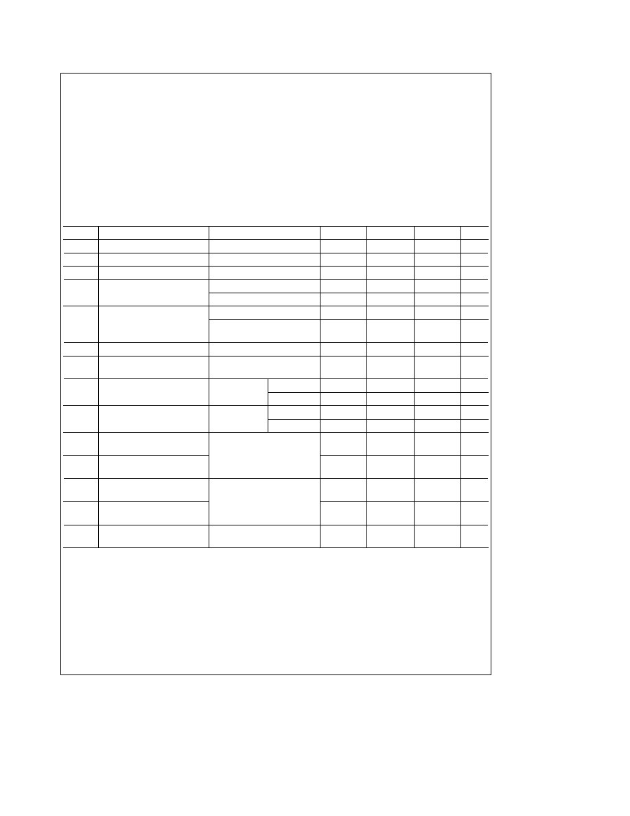
Absolute Maximum Ratings (Note 1)
If MilitaryAerospace specified devices are required
please contact the National Semiconductor Sales
OfficeDistributors for availability and specifications
Supply Voltage Range of VCC1 (Note 1)
b
05 to 7V
Supply Voltage Range of VCC2
b
05V to 25V
Input Voltage
55V
Inter-Input Voltage (Note 4)
55V
Storage Temperature Range
b
65 Cto a150 C
Maximum Power Dissipation at 25 C
Molded Package
1022 mW
Lead Temperature 116 inch from Case for
10 Seconds N or P Package
200 C
Derate molded package 82 mW
above about 25 C
Operating Conditions
Min
Max
Units
Supply Voltage (VCC1)
475
525
V
Supply Voltage (VCC2)
475
24
V
Operating Temperature (TA)0
a
70
C
Electrical Characteristics (Notes 2 and 3)
Symbol
Parameter
Conditions
Min
Typ
Max
Units
VIH
High-Level Input Voltage
2
V
VIL
Low-Level Input Voltage
08
V
VI
Input Clamp Voltage
II eb12 mA
b
15
V
VOH
High-Level Output Voltage
VIL e 08V IOH eb50 mAVCC2 b 1VCC2 b 07
V
VIL e 08V IOH eb10 mA
VCC2 b 23
VCC2 b 18
V
VOL
Low-Level Output Voltage
VIH e 2V IOL e 10 mA
015
03
V
VCC2 e 15V to 24V VIH e 2V
025
05
V
IOL e 40 mA
VO
Output Clamp Voltage
VI e 0V IOH e 20 mA
VCC2 a 15
V
II
Input Current at Maximum
VI e 55V
1
mA
Input Voltage
IIH
High-Level Input Current
VI e 24V
A Inputs
40
m
A
E Input
80
m
A
IIL
Low-Level Input Current
VI e 04V
A Inputs
b
1
b
16
mA
E Input
b
2
b
32
mA
ICC1(H)
Supply Current from VCC1 Both
24
mA
Outputs High
VCC1 e 525V
VCC2 e 24V
ICC2(H)
Supply Current from VCC2 Both
All Inputs at 0V
No Load
05
mA
Outputs High
ICC1(L)
Supply Current from VCC1 Both
16
24
mA
Outputs Low
VCC1 e 525V
VCC2 e 24V
ICC2(L)
Supply Current from VCC2 Both
All Inputs at 5V
No Load
711
mA
Outputs Low
ICC2(S)
Supply Current from VCC2
VCC1 e 0V
VCC2 e 24V
05
mA
Stand-by Condition
All Inputs at 5V
No Load
Note 1
‘‘Absolute Maximum Ratings’’ are those values beyond which the safety of the device cannot be guaranteed Except for ‘‘Operating Temperature Range’’
they are not meant to imply that the devices should be operated at these limits The table of ‘‘Electrical Characteristics’’ provides conditions for actual device
operation
Note 2
Unless otherwise specified minmax limits apply across the 0 Cto a70 C range for the DS75361 All typical values are for TA e 25 C and VCC1 e 5V and
VCC2 e 20V
Note 3
All currents into device pins shown as positive out of device pins as negative all voltages referenced to ground unless otherwise noted All values shown
as max or min on absolute value basis
Note 4
This rating applies between the A input of either driver and the common E input
2
相關(guān)PDF資料 |
PDF描述 |
|---|---|
| DSC-10510-193 | DIGITAL TO SYNCHRO OR RESOLVER, DMA40 |
| DSC-10510-163S | DIGITAL TO SYNCHRO OR RESOLVER, DMA40 |
| DSC5031-29HB | DIGITAL TO SYNCHRO OR RESOLVER, XMA26 |
| DSC5131-249SS | DIGITAL TO SYNCHRO OR RESOLVER, XMA26 |
| DSLU304 | DC-DC REG PWR SUPPLY MODULE |
相關(guān)代理商/技術(shù)參數(shù) |
參數(shù)描述 |
|---|---|
| DS75361J-8/A+ | 制造商:未知廠家 制造商全稱:未知廠家 功能描述:TTL-to-MOS Translator |
| DS75361N | 制造商:Texas Instruments 功能描述: |
| DS75361N/A+ | 制造商:未知廠家 制造商全稱:未知廠家 功能描述:TTL-to-MOS Translator |
| DS75361N-8/A+ | 制造商:未知廠家 制造商全稱:未知廠家 功能描述:TTL-to-MOS Translator |
| DS75361N-8/B+ | 制造商:未知廠家 制造商全稱:未知廠家 功能描述:TTL-to-MOS Translator |
發(fā)布緊急采購,3分鐘左右您將得到回復(fù)。