- 您現(xiàn)在的位置:買賣IC網 > PDF目錄1915 > DS26519GN+ (Maxim Integrated Products)IC TXRX T1/E1/J1 16PRT 484-HSBGA PDF資料下載
參數資料
| 型號: | DS26519GN+ |
| 廠商: | Maxim Integrated Products |
| 文件頁數: | 214/310頁 |
| 文件大?。?/td> | 0K |
| 描述: | IC TXRX T1/E1/J1 16PRT 484-HSBGA |
| 產品培訓模塊: | Lead (SnPb) Finish for COTS Obsolescence Mitigation Program |
| 標準包裝: | 30 |
| 類型: | 收發(fā)器 |
| 驅動器/接收器數: | 16/16 |
| 規(guī)程: | 以太網 |
| 電源電壓: | 3.135 V ~ 3.465 V |
| 安裝類型: | 表面貼裝 |
| 封裝/外殼: | 484-BGA 裸露焊盤 |
| 供應商設備封裝: | 484-HSBGA(23x23) |
| 包裝: | 管件 |
第1頁第2頁第3頁第4頁第5頁第6頁第7頁第8頁第9頁第10頁第11頁第12頁第13頁第14頁第15頁第16頁第17頁第18頁第19頁第20頁第21頁第22頁第23頁第24頁第25頁第26頁第27頁第28頁第29頁第30頁第31頁第32頁第33頁第34頁第35頁第36頁第37頁第38頁第39頁第40頁第41頁第42頁第43頁第44頁第45頁第46頁第47頁第48頁第49頁第50頁第51頁第52頁第53頁第54頁第55頁第56頁第57頁第58頁第59頁第60頁第61頁第62頁第63頁第64頁第65頁第66頁第67頁第68頁第69頁第70頁第71頁第72頁第73頁第74頁第75頁第76頁第77頁第78頁第79頁第80頁第81頁第82頁第83頁第84頁第85頁第86頁第87頁第88頁第89頁第90頁第91頁第92頁第93頁第94頁第95頁第96頁第97頁第98頁第99頁第100頁第101頁第102頁第103頁第104頁第105頁第106頁第107頁第108頁第109頁第110頁第111頁第112頁第113頁第114頁第115頁第116頁第117頁第118頁第119頁第120頁第121頁第122頁第123頁第124頁第125頁第126頁第127頁第128頁第129頁第130頁第131頁第132頁第133頁第134頁第135頁第136頁第137頁第138頁第139頁第140頁第141頁第142頁第143頁第144頁第145頁第146頁第147頁第148頁第149頁第150頁第151頁第152頁第153頁第154頁第155頁第156頁第157頁第158頁第159頁第160頁第161頁第162頁第163頁第164頁第165頁第166頁第167頁第168頁第169頁第170頁第171頁第172頁第173頁第174頁第175頁第176頁第177頁第178頁第179頁第180頁第181頁第182頁第183頁第184頁第185頁第186頁第187頁第188頁第189頁第190頁第191頁第192頁第193頁第194頁第195頁第196頁第197頁第198頁第199頁第200頁第201頁第202頁第203頁第204頁第205頁第206頁第207頁第208頁第209頁第210頁第211頁第212頁第213頁當前第214頁第215頁第216頁第217頁第218頁第219頁第220頁第221頁第222頁第223頁第224頁第225頁第226頁第227頁第228頁第229頁第230頁第231頁第232頁第233頁第234頁第235頁第236頁第237頁第238頁第239頁第240頁第241頁第242頁第243頁第244頁第245頁第246頁第247頁第248頁第249頁第250頁第251頁第252頁第253頁第254頁第255頁第256頁第257頁第258頁第259頁第260頁第261頁第262頁第263頁第264頁第265頁第266頁第267頁第268頁第269頁第270頁第271頁第272頁第273頁第274頁第275頁第276頁第277頁第278頁第279頁第280頁第281頁第282頁第283頁第284頁第285頁第286頁第287頁第288頁第289頁第290頁第291頁第292頁第293頁第294頁第295頁第296頁第297頁第298頁第299頁第300頁第301頁第302頁第303頁第304頁第305頁第306頁第307頁第308頁第309頁第310頁
DS26519 16-Port T1/E1/J1 Transceiver
291 of 310
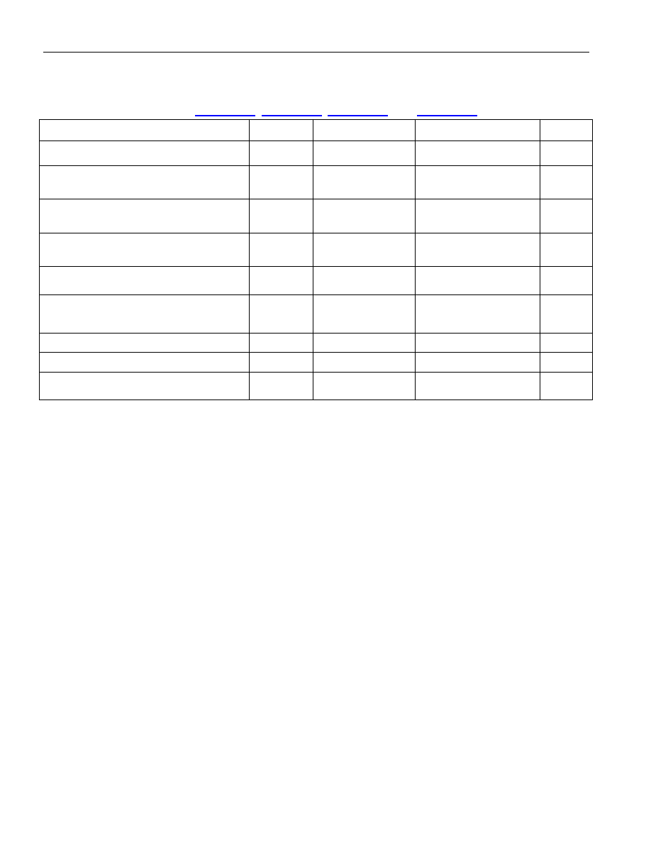
Table 13-2. AC Characteristics—Microprocessor Bus Timing
(VDD = 3.3V ±5%, TA = 0°C to +70°C for DS26519G; VDD = 3.3V ±5%, TA = -40°C to +85°C for
PARAMETER
SYMBOL
CONDITIONS
MIN
TYP
MAX
UNITS
Setup Time for A[13:0] Valid to
CSB
Active
t1
0
ns
Setup Time for
CSB Active to Either RDB,
or
WRB Active
t2
0
ns
Delay Time from Either
RDB or DSB
Active to D[7:0] Valid
t3
(Note 2)
175
ns
Hold Time from Either
RDB or WRB
Inactive to
CSB Inactive
t4
0
ns
Hold Time from
CSB or RDB or DSB
Inactive to D[7:0] Tri-State
t5
5
20
ns
Wait Time from
WRB Active to Latch Data
t6
40
ns
Data Setup Time to
WRB Inactive
t7
10
ns
Data Hold Time from
WRB Inactive
t8
2
ns
Address Hold from
WRB Inactive
t9
0
ns
Write Access to Subsequent Write/Read
Access Delay Time
t10
(Note 2)
30
ns
Note 1:
The timing parameters in this table are guaranteed by design (GBD).
Note 2:
If supplying a 1.544MHz MCLK, the FREQSEL bit must be set to meet this timing.
相關PDF資料 |
PDF描述 |
|---|---|
| DS26521L+ | IC TXRX T1/E1/J1 64-LQFP |
| DS26522GN+ | IC TXRX T1/E1/J1 DUAL 144CSBGA |
| DS26524GNA5+ | IC TXRX T1/E1/J1 QUAD 256-CSBGA |
| DS26528GNA5+ | IC TXRX T1/E1/J1 OCT 256-CSBGA |
| DS26900LN+ | IC JTAG MUX/SWITCH 144-LQFP |
相關代理商/技術參數 |
參數描述 |
|---|---|
| DS26519GN+ | 功能描述:網絡控制器與處理器 IC 16-Port E1/T1/J1 Transceiver RoHS:否 制造商:Micrel 產品:Controller Area Network (CAN) 收發(fā)器數量: 數據速率: 電源電流(最大值):595 mA 最大工作溫度:+ 85 C 安裝風格:SMD/SMT 封裝 / 箱體:PBGA-400 封裝:Tray |
| DS26519GNA2 | 功能描述:網絡控制器與處理器 IC 16-Port E1/T1/J1 Transceiver RoHS:否 制造商:Micrel 產品:Controller Area Network (CAN) 收發(fā)器數量: 數據速率: 電源電流(最大值):595 mA 最大工作溫度:+ 85 C 安裝風格:SMD/SMT 封裝 / 箱體:PBGA-400 封裝:Tray |
| DS26519GNA2+ | 功能描述:網絡控制器與處理器 IC 16-Port E1/T1/J1 Transceiver RoHS:否 制造商:Micrel 產品:Controller Area Network (CAN) 收發(fā)器數量: 數據速率: 電源電流(最大值):595 mA 最大工作溫度:+ 85 C 安裝風格:SMD/SMT 封裝 / 箱體:PBGA-400 封裝:Tray |
| DS26521 | 制造商:Maxim Integrated Products 功能描述:DS26521 MONOLITHIC T1E1J1 SCT - Rail/Tube |
| DS26521DK | 功能描述:網絡開發(fā)工具 DS26521 Dev Kit RoHS:否 制造商:Rabbit Semiconductor 產品:Development Kits 類型:Ethernet to Wi-Fi Bridges 工具用于評估:RCM6600W 數據速率:20 Mbps, 40 Mbps 接口類型:802.11 b/g, Ethernet 工作電源電壓:3.3 V |
發(fā)布緊急采購,3分鐘左右您將得到回復。