- 您現(xiàn)在的位置:買賣IC網(wǎng) > PDF目錄93261 > DS2188SN (DALLAS SEMICONDUCTOR) DATACOM, PCM JITTER ATTENUATOR, PDSO16 PDF資料下載
參數(shù)資料
| 型號: | DS2188SN |
| 廠商: | DALLAS SEMICONDUCTOR |
| 元件分類: | Digital Transmission Interface |
| 英文描述: | DATACOM, PCM JITTER ATTENUATOR, PDSO16 |
| 封裝: | SOIC-16 |
| 文件頁數(shù): | 5/10頁 |
| 文件大小: | 137K |
| 代理商: | DS2188SN |
DS2188
4 of 10
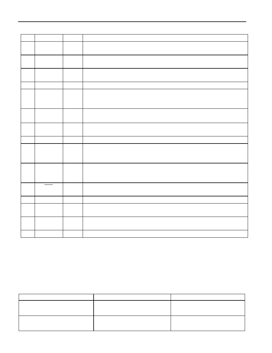
PIN DESCRIPTION Table 1
PIN
SYMBOL
TYPE
DESCRIPTION
1DJA
I
Disable Jitter Attenuation. When high, jittered data and clock at RPOS,
RNEG, and RCLK are passed directly to RRPOS, RRNEG, and RRCLK.
2RPOS
I
Receive Positive Data Input. Jittered data input. Sampled on the falling
edge of RCLK.
3RNEG
I
Receive Negative Data Input. Jittered data input. Sampled on the falling
edge of RCLK.
4
RCLK
I
Receive Clock Input. Jittered input 1.544 MHz or 2.048 MHz clock.
5BDS
I
Buffer Depth Select.
0 = 128 bits
1 = 32 bits
6
TEST
I
Test Input. In normal applications, this pin should be tied low.
When tied high, used to verify free running frequency of XTAL.
7XTAL
OUT
O
Crystal Frequency Output. Buffered output of the 4X crystal connected
to XTAL1 and XTAL2.
8VSS
-
Ground. 0.0V
9
10
XTAL1
XTAL2
I
O
Crystal Connections. In T1 environments, connect a 6.176 MHz crystal
to these pins. In CEPT environments, connect an 8.192 MHz crystal to
these pins.
11
BL
O
Buffer Limit. Transitions high when the buffer fills or empties to within
either 4 bits (BDS=0) or 2 bits (BDS=1) of its capacity. Indicates that the
jitter at RCLK is greater than 120 UIpp (BDS=0) or 28 UIpp (BDS=1).
12
RST
I
Reset. Negative-edge triggered; a high-low transition will recenter the
buffer. Activation of this pin may corrupt data through the DS2188.
13
RRCLK
O
Receive Reference Clock. Dejittered 1.544 MHz or 2.048 MHz clock.
14
RRNEG
O
Receive Reference Negative Data Output. Dejittered data output.
Updated on the rising edge of RRCLK.
15
RRPOS
O
Receive Reference Positive Data Output. Dejittered data output.
Updated on the rising edge of RRCLK.
16
VDD
-
Positive Supply. 5.0V
CRYSTAL REQUIREMENTS
The DS2188 must have a crystal connected to the XTAL1 and XTAL2 pins. For T1 environments, the
frequency of this crystal should be 6.176 MHz. For CEPT environments, the frequency of this crystal
should be 8.192 MHz. Table 2 lists some suggested crystal manufacturers that are recommended for use
with the DS2188. Also, see DS2188 Application Note, “Operation at Speeds Greater than E1” for
additional information.
CRYSTAL MANUFACTURERS Table 2
MANUFACTURER
PART #
FREQUENCY
JAN Crystal
6323-00, JC6A14
6323-00, JC8A14
6.176 MHz
8.192 MHz
M-TRON
4575-002
4575-001
6.176 MHz
8.192 MHz
相關PDF資料 |
PDF描述 |
|---|---|
| DS2188 | DATACOM, PCM JITTER ATTENUATOR, PDIP16 |
| DS2188S | DATACOM, PCM JITTER ATTENUATOR, PDSO16 |
| DS21Q554 | DATACOM, PCM TRANSCEIVER, PBGA256 |
| DS21S07AS | 9-LINE 110 ohm SCSI BUS TERMINATOR, PDSO16 |
| DS21S07AE | 9-LINE 110 ohm SCSI BUS TERMINATOR, PDSO20 |
相關代理商/技術參數(shù) |
參數(shù)描述 |
|---|---|
| DS2188SN/T&R | 制造商:Maxim Integrated Products 功能描述:JITTER ATTENUATOR-SOIC-IND TRL - Tape and Reel |
| DS2188SN/T&R | 功能描述:通信集成電路 - 若干 RoHS:否 制造商:Maxim Integrated 類型:Transport Devices 封裝 / 箱體:TECSBGA-256 數(shù)據(jù)速率:100 Mbps 電源電壓-最大:1.89 V, 3.465 V 電源電壓-最小:1.71 V, 3.135 V 電源電流:50 mA, 225 mA 最大工作溫度:+ 85 C 最小工作溫度:- 40 C 封裝:Tube |
| DS2188SN/TRL | 功能描述:IC ATTEN JTR T1/CEPT IND 16-SOIC RoHS:否 類別:集成電路 (IC) >> 專用 IC 系列:- 產(chǎn)品培訓模塊:Lead (SnPb) Finish for COTS Obsolescence Mitigation Program 標準包裝:1 系列:- 類型:調(diào)幀器 應用:數(shù)據(jù)傳輸 安裝類型:表面貼裝 封裝/外殼:400-BBGA 供應商設備封裝:400-PBGA(27x27) 包裝:散裝 |
| DS2188SN+ | 功能描述:通信集成電路 - 若干 RoHS:否 制造商:Maxim Integrated 類型:Transport Devices 封裝 / 箱體:TECSBGA-256 數(shù)據(jù)速率:100 Mbps 電源電壓-最大:1.89 V, 3.465 V 電源電壓-最小:1.71 V, 3.135 V 電源電流:50 mA, 225 mA 最大工作溫度:+ 85 C 最小工作溫度:- 40 C 封裝:Tube |
| DS2188SN+T&R | 制造商:Maxim Integrated Products 功能描述:T1/CEPT JITTER ATTENUATOR 16SOIC W - Tape and Reel |
發(fā)布緊急采購,3分鐘左右您將得到回復。