- 您現(xiàn)在的位置:買賣IC網(wǎng) > PDF目錄67327 > DS1668 (MAXIM INTEGRATED PRODUCTS INC) 1 TIMER(S), REAL TIME CLOCK, PDIP28 PDF資料下載
參數(shù)資料
| 型號(hào): | DS1668 |
| 廠商: | MAXIM INTEGRATED PRODUCTS INC |
| 元件分類: | Timer or RTC |
| 英文描述: | 1 TIMER(S), REAL TIME CLOCK, PDIP28 |
| 封裝: | 0.600 INCH, DIP-28 |
| 文件頁(yè)數(shù): | 5/12頁(yè) |
| 文件大?。?/td> | 238K |
| 代理商: | DS1668 |
MAX541/MAX542
+5V, Serial-Input, Voltage-Output, 16-Bit DACs
2
_______________________________________________________________________________________
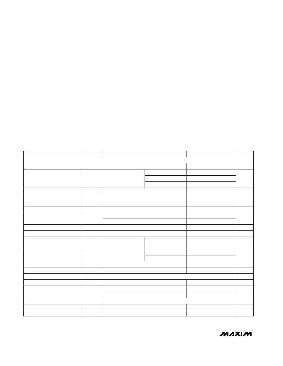
ABSOLUTE MAXIMUM RATINGS
ELECTRICAL CHARACTERISTICS
(VDD = +5V ±5%, VREF = +2.5V, AGND = DGND = 0, TA = TMIN to TMAX, unless otherwise noted.)
Stresses beyond those listed under “Absolute Maximum Ratings” may cause permanent damage to the device. These are stress ratings only, and functional
operation of the device at these or any other conditions beyond those indicated in the operational sections of the specifications is not implied. Exposure to
absolute maximum rating conditions for extended periods may affect device reliability.
VDD to DGND ...........................................................-0.3V to +6V
CS, SCLK, DIN, LDAC to DGND ..............................-0.3V to +6V
REF, REFF, REFS to AGND ........................-0.3V to (VDD + 0.3V)
AGND, AGNDF, AGNDS to DGND........................-0.3V to +0.3V
OUT, INV to AGND, DGND ......................................-0.3V to VDD
RFB to AGND, DGND..................................................-6V to +6V
Maximum Current into Any Pin............................................50mA
Continuous Power Dissipation (TA = +70°C)
8-Pin Plastic DIP (derate 9.09mW/°C above +70°C) .....727mW
8-Pin SO (derate 5.88mW/°C above +70°C) .................471mW
14-Pin Plastic DIP (derate 10.00mW/°C above +70°C) ...800mW
14-Pin SO (derate 8.33mW/°C above +70°C) ...............667mW
14-Pin Ceramic SB (derate 10.00mW/°C above +70°C ..800mW
Operating Temperature Ranges
MAX541 _C_ A/MAX542_C_D. .............................0°C to +70°C
MAX541 _E_ A/MAX542_E_D............................-40°C to +85°C
MAX542CMJD .................................................-55°C to +125°C
Storage Temperature Range .............................-65°C to +150°C
Lead Temperature (soldering, 10s) .................................+300°C
MAX542, bipolar mode
Unipolar mode
(Note 3)
4.75V
≤ VDD ≤ 5.25V
MAX542
TA = TMIN to TMAX
TA = +25°C
Ratio error
TA = +25°C
TA = TMIN to TMAX
VDD = 5V
TA = +25°C
RFB/RINV
TA = TMIN to TMAX
(Note 2)
CONDITIONS
k
9.0
RREF
Reference Input Resistance
(Note 4)
11.5
V
2.0
3.0
VREF
Reference Input Range
PSR
Power-Supply Rejection
LSB
±1.0
ppm/°C
±0.5
BZSTC
Bipolar Zero Tempco
LSB
±10
±0.015
Bipolar Resistor Matching
1.0
ROUT
DAC Output Resistance
k
6.25
±0.5
±1.0
Bits
16
N
Resolution
ppm/°C
±0.1
Gain-Error Tempco
LSB
±10
Gain Error (Note 1)
±5
ppm/°C
±0.05
ZSTC
Zero-Code Tempco
LSB
±0.5
±2.0
INL
Integral Nonlinearity
±0.5
±4.0
±1
±2
Zero-Code Offset Error
UNITS
MIN
TYP
MAX
SYMBOL
PARAMETER
ZSE
LSB
MAX54_A
MAX54_B
TA = TMIN to TMAX
±20
Bipolar Zero Offset Error
CL = 10pF (Note 5)
25
V/s
SR
Voltage-Output Slew Rate
DYNAMIC PERFORMANCE—ANALOG SECTION (RL =
∞, unipolar mode)
to ±1/2LSB of FS, CL = 10pF
1
s
Output Settling Time
Guaranteed monotonic
LSB
±0.5
±1.0
DNL
Differential Nonlinearity
MAX54_C
STATIC PERFORMANCE—ANALOG SECTION (RL =
∞)
REFERENCE INPUT
MAX542
%
相關(guān)PDF資料 |
PDF描述 |
|---|---|
| 5962-8961603VX | 1-CH 8-BIT SUCCESSIVE APPROXIMATION ADC, PARALLEL ACCESS, CDIP18 |
| 5962-8961604VX | 1-CH 8-BIT SUCCESSIVE APPROXIMATION ADC, PARALLEL ACCESS, CDIP18 |
| 5962-8962001PA | 1 CHANNEL, VIDEO AMPLIFIER, CDIP8 |
| 5962-8963701CX | RMS TO DC CONVERTER, 0.15 MHz, CDIP14 |
| 5962-8965701LX | DUAL, PARALLEL, WORD INPUT LOADING, 12-BIT DAC, CDIP24 |
相關(guān)代理商/技術(shù)參數(shù) |
參數(shù)描述 |
|---|---|
| DS1668S10 | 制造商:未知廠家 制造商全稱:未知廠家 功能描述:Interface IC |
| DS1668S100 | 制造商:未知廠家 制造商全稱:未知廠家 功能描述:Interface IC |
| DS1668S50 | 制造商:未知廠家 制造商全稱:未知廠家 功能描述:Interface IC |
| DS1669 | 制造商:DALLAS 制造商全稱:Dallas Semiconductor 功能描述:Dallastat Electronic Digital Rheostat |
| DS1669-010 | 制造商:DALLAS 制造商全稱:Dallas Semiconductor 功能描述:Dallastat Electronic Digital Rheostat |
發(fā)布緊急采購(gòu),3分鐘左右您將得到回復(fù)。