- 您現(xiàn)在的位置:買賣IC網(wǎng) > PDF目錄379176 > DS1000-75 RECTIFIER BRIDGE 1A 400V DB-1 PDF資料下載
參數(shù)資料
| 型號(hào): | DS1000-75 |
| 英文描述: | RECTIFIER BRIDGE 1A 400V DB-1 |
| 中文描述: | 5抽頭硅延遲線 |
| 文件頁(yè)數(shù): | 3/5頁(yè) |
| 文件大小: | 65K |
| 代理商: | DS1000-75 |
DS1000
3 of 5
CAPACITANCE
PARAMETER
Input Capacitance
(T
A
= 25°C)
UNITS
pF
SYMBOL
C
IN
MIN
TYP
5
MAX
10
NOTES
NOTES:
1.
Initial tolerances are
±
=
with respect to the nominal value at 25
°
C and 5V.
2.
Temperature tolerance is
±
=
with respect to the initial delay value over a range of 0
°
C to 70
°
C.
3.
The delay will also vary with supply voltage, typically by less than 4% over the range 4.75 to 5.25V.
4.
All tap delays tend to vary uni-directionally with temperature or voltage changes. For example, if
TAP 1 slows down, all other taps also slow down; TAP3 can never be faster than TAP2.
5.
Intermediate delay values and packaging variations are available on a custom basis. For further
information, call 972-371–4348.
6.
All voltages are referenced to ground.
7.
Measured with outputs open.
8.
Pulse width and period specifications may be exceeded; however, accuracy may be impaired
depending on application (decoupling, layout, etc.). The device will remain functional with pulse
widths down to 20% of Tap 5 delay, and input periods as short as 2(t
WI
).
9.
I
CC
is a function of frequency and TAP 5 delay. Only a -25 operating with a 40-ns period and V
CC
=
5.25V will have an I
CC
= 75 mA. For example a -100 will never exceed 30 mA, etc.
10.
See “Test Conditions” section at the end of this data sheet.
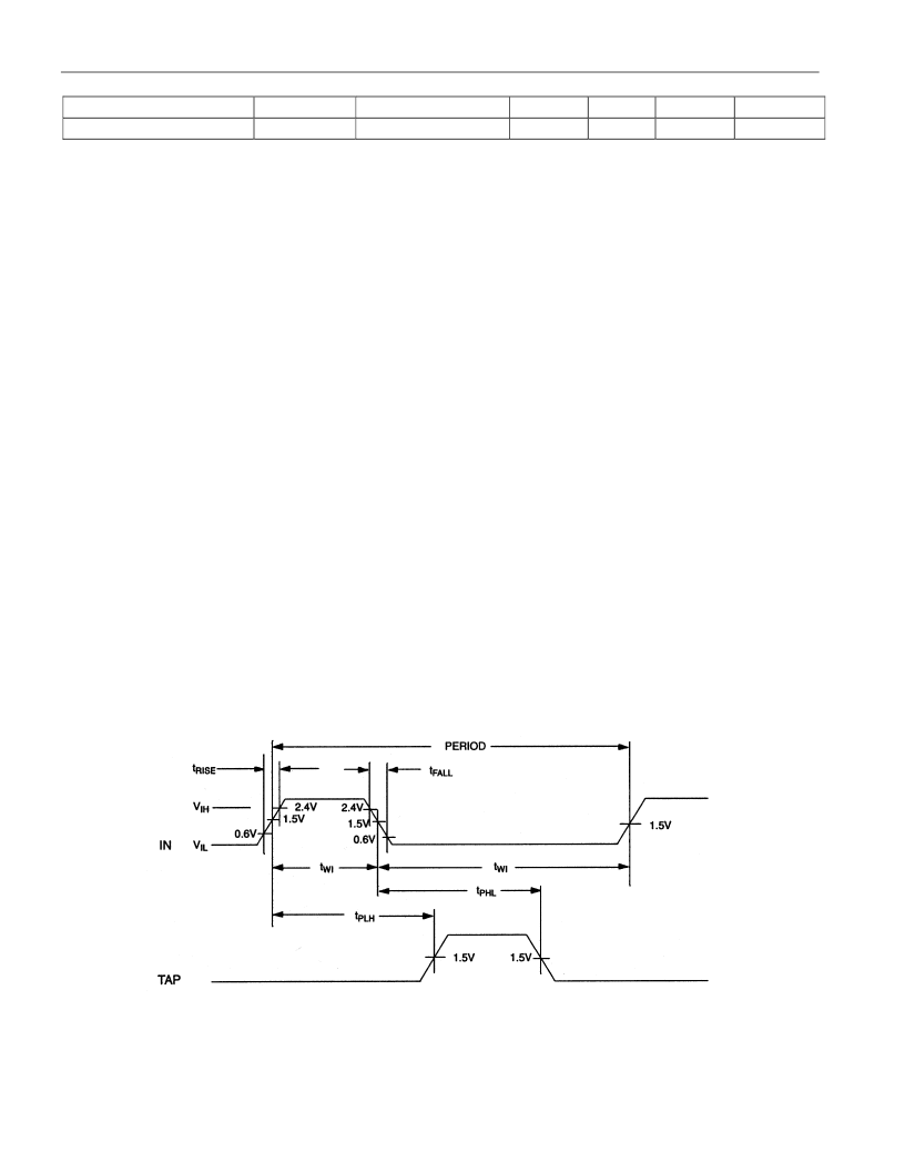
TIMING DIAGRAM: SILICON DELAY LINE
Figure 2
相關(guān)PDF資料 |
PDF描述 |
|---|---|
| DS106C2 | Fixed Inductors for Surface Mounting |
| DS1073Z-80 | 3V EconOscillator/Divider |
| DS1073Z-100 | 3V EconOscillator/Divider |
| DS1073 | EconOscillator/Divider |
| DS1073M-60 | 3V EconOscillator/Divider |
相關(guān)代理商/技術(shù)參數(shù) |
參數(shù)描述 |
|---|---|
| DS1000-75IND | 制造商:未知廠家 制造商全稱:未知廠家 功能描述:Tapped Delay Line |
| DS1000C209 | 制造商:DAL+E1361 功能描述:* |
| DS1000C-209 | 制造商:Maxim Integrated Products 功能描述:1000C-209 |
| DS1000C-302/T&R/ | 制造商:Rochester Electronics LLC 功能描述: 制造商:Maxim Integrated Products 功能描述: |
| DS1000C311 | 制造商:DALLAS 功能描述:New |
發(fā)布緊急采購(gòu),3分鐘左右您將得到回復(fù)。