- 您現(xiàn)在的位置:買賣IC網(wǎng) > PDF目錄382942 > DFLU1200-7 (DIODES INC) 1.0A SURFACE MOUNT SUPER-FAST RECTIFIER PDF資料下載
參數(shù)資料
| 型號(hào): | DFLU1200-7 |
| 廠商: | DIODES INC |
| 元件分類: | 參考電壓二極管 |
| 英文描述: | 1.0A SURFACE MOUNT SUPER-FAST RECTIFIER |
| 中文描述: | 1 A, 200 V, SILICON, SIGNAL DIODE |
| 封裝: | GREEN, PLASTIC, POWERDI 123, 2 PIN |
| 文件頁數(shù): | 1/3頁 |
| 文件大?。?/td> | 108K |
| 代理商: | DFLU1200-7 |
e
3
DS30601 Rev. 2 - 2
1 of 3
DFLU1200
PowerDI is a trademark of Diodes Incorporated.
www.diodes.com
Diodes Incorporated
DFLU1200
1.0A SURFACE MOUNT SUPER-FAST RECTIFIER
PowerDI
123
Features
Maximum Ratings and Electrical Characteristics
Single phase, half wave, 60Hz, resistive or inductive load.
For capacitive load, derate current by 20%.
T
A
= 25 C unless otherwise specified
Glass Passivated Die Construction
Super-Fast Recovery Time for High Efficiency
Low Forward Voltage Drop and High Current Capability
Lead Free Finish, RoHS Compliant (Note 2)
Green Molding Compound (No Br, Sb)
Qualified to AEC-Q101 Standards for High Reliability
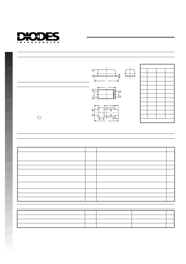
Mechanical Data
N
B
A
A
C
E
L4
L
L1
E
H
D
L3
L2
L
PowerDI 123
Min
3.50
2.60
1.63
0.93
0.85
0.15
0.45
—
—
—
0.90
All Dimensions in mm
Dim
A
B
C
D
E
H
L
L1
L2
L3
L4
Max
3.90
3.00
1.93
1.00
1.25
0.25
0.85
—
—
—
1.30
Typ
3.70
2.80
1.78
0.98
1.00
0.20
0.65
1.35
1.10
0.20
1.05
Case: PowerDI 123
Case Material: Molded Plastic, "Green" Molding
Compound. UL Flammability Classification Rating
94V-0
Moisture sensitivity: Level 1 per J-STD-020C
Terminal Connections: Cathode Band
Terminals: Finish – Matte Tin annealed over Copper
leadframe. Solderable per MIL-STD-202,
Method 208
Marking & Type Code Information: See Last Page
Ordering Information: See Last Page
Weight: 0.01 grams (approximate)
Notes: 1. Device mounted on 1" x 1", Polymide PCB; 2 oz. Cu pad layout as shown on Diodes Inc. suggested pad layout document AP02001.pdf.
2. RoHS revision 13.2.2003. Glass and High Temperature Solder Exemptions Applied, see EU Directive Annex Notes 5 and 7
3. Theoretical R
JS
calculated from the top center of the die straight down to the PCB cathode tab solder junction.
4. Measured with I
F
= 0.5A, I
R
= 1.0A, I
rr
= 0.25A. See figure 5.
5. Short duration pulse test to minimize self-heating effect.
Characteristic
Symbol
V
RRM
V
RWM
V
R
V
R(RMS)
I
O
DFLU1200
Unit
Peak Repetitive Reverse Voltage
Working Peak Reverse Voltage
DC Blocking Voltage
RMS Reverse Voltage
Average Rectified Output Current
Non-Repetitive Peak Forward Surge Current
8.3ms Single half sine-wave Superimposed on Rated Load
Forward Voltage Drop (Note 5)
200
V
140
1.0
V
A
I
FSM
30
A
@ I
F
= 0.6A
@ I
F
= 1.0A
@ T
A
= 25 C
@ T
A
= 100 C
V
FM
0.90
0.98
5.0
200
V
Peak Reverse Current
at Rated DC Blocking Voltage (Note 5)
Reverse Recovery Time (Note 4)
Typical Total Capacitance (f = 1MHz, V
R
= 4VDC)
Operating and Storage Temperature Range
I
RM
A
t
rr
C
T
25
27
ns
pF
C
T
j,
T
STG
-65 to +150
Thermal Characteristics
@ T
A
= 25 C unless otherwise specified
Characteristic
Symbol
P
D
R
JA
R
JS
Typ
Max
1.0
Unit
W
°C/W
°C/W
Power Dissipation (Note 1)
Thermal Resistance Junction to Ambient (Note 1)
Thermal Resistance Junction to Soldering (Note 3)
116
6
相關(guān)PDF資料 |
PDF描述 |
|---|---|
| DFLU1400 | 1.0A SURFACE MOUNT SUPER-FAST RECTIFIER |
| DFLU1400-7 | 1.0A SURFACE MOUNT SUPER-FAST RECTIFIER |
| DFLZ10 | 1.0W SURFACE MOUNT POWER ZENER DIODE |
| DFLZ10-7 | 1.0W SURFACE MOUNT POWER ZENER DIODE |
| DFLZ11 | 1.0W SURFACE MOUNT POWER ZENER DIODE |
相關(guān)代理商/技術(shù)參數(shù) |
參數(shù)描述 |
|---|---|
| DFLU1400 | 制造商:DIODES 制造商全稱:Diodes Incorporated 功能描述:1.0A SURFACE MOUNT SUPER-FAST RECTIFIER |
| DFLU1400_1 | 制造商:DIODES 制造商全稱:Diodes Incorporated 功能描述:1.0A SURFACE MOUNT SUPER-FAST RECTIFIER |
| DFLU1400-7 | 功能描述:整流器 RECTIFIER SUPERFAST PWRDI 1.0A 400V RoHS:否 制造商:Vishay Semiconductors 產(chǎn)品:Standard Recovery Rectifiers 配置: 反向電壓:100 V 正向電壓下降: 恢復(fù)時(shí)間:1.2 us 正向連續(xù)電流:2 A 最大浪涌電流:35 A 反向電流 IR:5 uA 安裝風(fēng)格:SMD/SMT 封裝 / 箱體:DO-221AC 封裝:Reel |
| DFLU1400-7-F | 制造商:Zetex / Diodes Inc 功能描述:RECTIFIER SUPERFAST GPP POWERD |
| DFLU1600-7 | 制造商:Diodes Incorporated 功能描述:RECTIFIER 1A SURFACE MOUNT SUPER-FAST RE PDI-123 1A SM - Tape and Reel |
發(fā)布緊急采購,3分鐘左右您將得到回復(fù)。