- 您現(xiàn)在的位置:買賣IC網(wǎng) > PDF目錄378536 > DDC114TK (Diodes Inc.) NPN PRE-BIASED SMALL SIGNAL SOT-26 DUAL SURFACE MOUNT TRANSISTOR PDF資料下載
參數(shù)資料
| 型號(hào): | DDC114TK |
| 廠商: | Diodes Inc. |
| 英文描述: | NPN PRE-BIASED SMALL SIGNAL SOT-26 DUAL SURFACE MOUNT TRANSISTOR |
| 中文描述: | npn型預(yù)偏置信號(hào)小的SOT - 26表面貼裝晶體管雙 |
| 文件頁數(shù): | 11/30頁 |
| 文件大小: | 389K |
| 代理商: | DDC114TK |
第1頁第2頁第3頁第4頁第5頁第6頁第7頁第8頁第9頁第10頁當(dāng)前第11頁第12頁第13頁第14頁第15頁第16頁第17頁第18頁第19頁第20頁第21頁第22頁第23頁第24頁第25頁第26頁第27頁第28頁第29頁第30頁
""#
SBAS255A JUNE 2004 REVISED NOVEMBER 2004
www.ti.com
11
At the completion of an A/D conversion, the charge on the
integration capacitor (C
F
) is reset with S
REF1
and
S
RESET
(see Figure 4 and Figure 5a). This is done during the reset
time. In this manner, the selected capacitor is charged to
the reference voltage, VREF. Once the integration
capacitor is charged, S
REF1
, and S
RESET
are switched so
that VREF is no longer connected to the amplifier circuit
while it waits to begin integrating (see Figure 5b). With the
rising edge on CONV, S
INTA
closes, which begins the
integration of Channel A. This process puts the integrator
stage into its integrate mode (see Figure 5c).
Charge from the input signal is collected on the integration
capacitor causing the voltage output of the amplifier to
decrease. A falling edge CONV stops the integration by
switching the input signal from side A to side B (S
INTA
and
S
INTB
). Prior to the falling edge of CONV, the signal on side
B was converted by the A/D converter and reset during the
time that side A was integrating. With the falling edge of
CONV, side B starts integrating the input signal. Now the
output voltage of side A’s operational amplifier is
presented to the input of the
Σ
A/D converter (see
Figure 5d).
Integration Capacitors
There are seven different capacitors available on-chip for
each side of each channel in the DDC114. These internal
capacitors are trimmed in production to achieve the
specified performance for range error of the DDC114. The
range control pins (RANGE0-RANGE2) change the
capacitor value for all four integrators. Consequently, both
inputs and both sides of each input will always have the
same full-scale range. Table 1 shows the capacitor value
selected for each range selection.
Table 1. Range Selection of the DDC114
RANGE2
RANGE1
RANGE0
(pCF
INPUT RANGE
(pC, typ)
0
0
0
0
1
1
1
1
0
0
1
1
0
0
1
1
0
1
0
1
0
1
0
1
3
0.048 to 12
–0.2 to 50
–0.4 to 100
–0.6 to 150
–0.8 to 200
–0.1 to 250
–1.2 to 300
–1.4 to 350
12.5
25
37.5
50
62.5
75
87.5
Voltage Reference
The external voltage reference is used to reset the
integration capacitors before an integration cycle begins.
It is also used by the
Σ
converter while the converter is
measuring the voltage stored on the integrators after an
integration cycle ends. During this sampling, the external
reference must supply the charge needed by the
Σ
converter. For an integration time of 400
μ
s, this charge
translates to an average VREF current of approximately
75
μ
A. The amount of charge needed by the
Σ
converter
is independent of the integration time; therefore,
increasing the integration time lowers the average current.
For example, an integration time of 800
μ
s lowers the
average VREF current to 37.5
μ
A.
It is critical that VREF be stable during the different modes
of operation (see Figure 5). The
Σ
converter measures
the voltage on the integrator with respect to VREF. Since
the integrator capacitors are initially reset to VREF, any
drop in VREF from the time the capacitors are reset to the
time when the converter measures the integrator output
will introduce an offset. It is also important that VREF be
stable over longer periods of time because changes in
VREF correspond directly to changes in the full-scale
range. Finally, VREF should introduce as little additional
noise as possible.
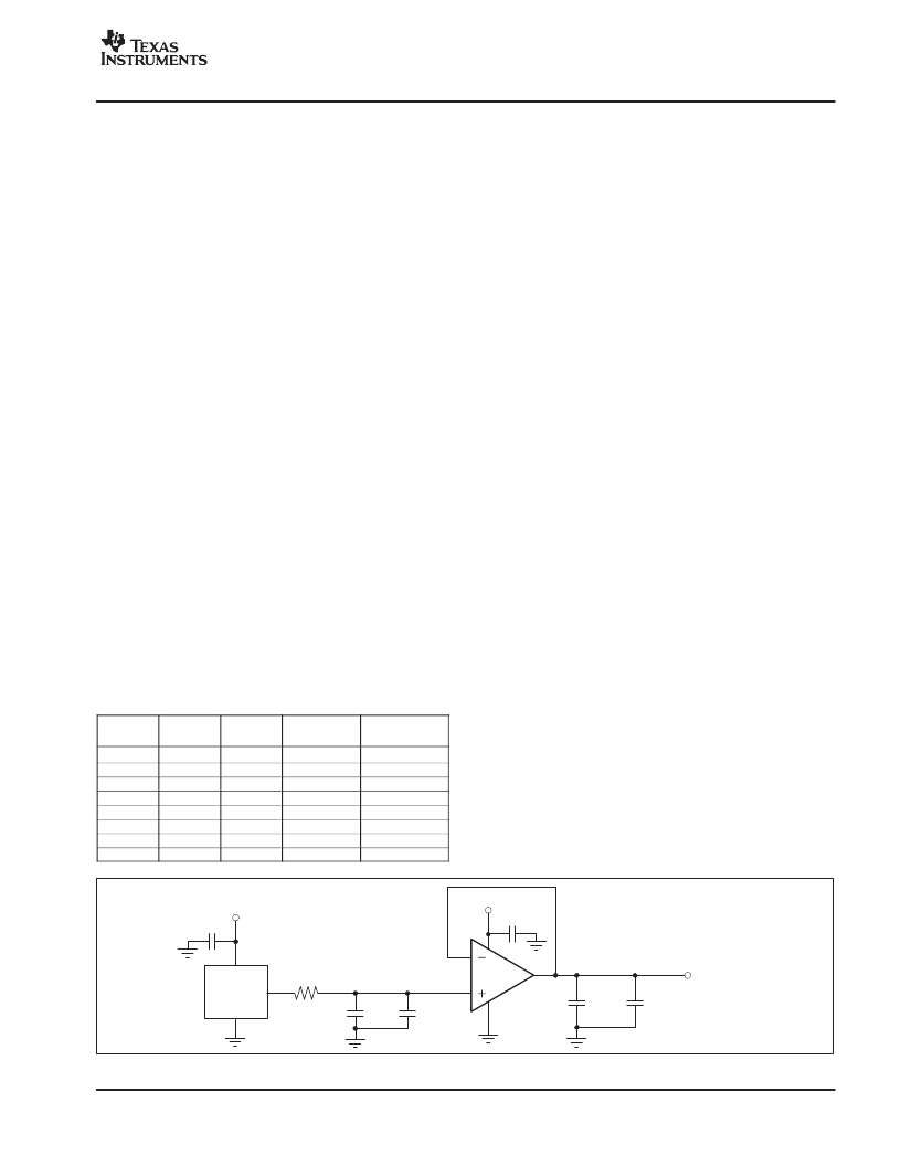
For these reasons, it is strongly recommended that the
external reference source be buffered with an operational
amplifier, as shown in Figure 6. In this circuit, the voltage
reference is generated by a 4.096V reference.
A low-pass
filter to reduce noise connects it to an operational amplifier
configured as a buffer. This amplifier should have a
unity-gain bandwidth greater than 4MHz, low noise, and
input/output common-mode ranges that support VREF.
Following the buffer are capacitors placed close to the
DDC114 VREF pin. Even though the circuit in Figure 6
might appear to be unstable due to the large output
capacitors, it works well for most operational amplifiers. It
is NOT recommended that series resistance be placed in
the output lead to improve stability since this can cause
drop in VREF, which produces large offsets.
0.10
μ
F
+5V
10k
10
μ
F
4
3
2
3
1
2
7
6
+
0.10
μ
F
0.1
μ
F
10
μ
F
+
OPA350
0.47
μ
F
+5V
To VREF
Pin 10 of
the DDC114
REF3140
Figure 6. Recommended External Voltage Reference Circuit for Best Low-Noise Operation with the DDC114
相關(guān)PDF資料 |
PDF描述 |
|---|---|
| DDC114YH | NPN PRE-BIASED SMALL SIGNAL SOT-563 DUAL SURFACE MOUNT TRANSISTOR |
| DDC114YK | NPN PRE-BIASED SMALL SIGNAL SOT-26 DUAL SURFACE MOUNT TRANSISTOR |
| DDC114EH | NPN PRE-BIASED SMALL SIGNAL SOT-563 DUAL SURFACE MOUNT TRANSISTOR |
| DDC114EH-7 | NPN PRE-BIASED SMALL SIGNAL SOT-563 DUAL SURFACE MOUNT TRANSISTOR |
| DDC114YK-7 | NPN PRE-BIASED SMALL SIGNAL SOT-26 DUAL SURFACE MOUNT TRANSISTOR |
相關(guān)代理商/技術(shù)參數(shù) |
參數(shù)描述 |
|---|---|
| DDC114TK-7 | 制造商:Diodes Incorporated 功能描述:TRANS DGTL BJT NPN 50V 100MA 6PIN SOT-26 - Tape and Reel |
| DDC114TK-7-F | 制造商:Diodes Incorporated 功能描述:PREBIASED TRANSISTOR SOT-26 R1 ONLY NPN 300MW 10KOHMS ROHS 3 - Tape and Reel |
| DDC114TU | 制造商:DIODES 制造商全稱:Diodes Incorporated 功能描述:NPN PRE-BIASED SMALL SIGNAL SOT-363 DUAL SURFACE MOUNT TRANSISTOR |
| DDC114TU-7 | 功能描述:開關(guān)晶體管 - 偏壓電阻器 DUAL NPN 200mW RoHS:否 制造商:ON Semiconductor 配置: 晶體管極性:NPN/PNP 典型輸入電阻器: 典型電阻器比率: 安裝風(fēng)格:SMD/SMT 封裝 / 箱體: 直流集電極/Base Gain hfe Min:200 mA 最大工作頻率: 集電極—發(fā)射極最大電壓 VCEO:50 V 集電極連續(xù)電流:150 mA 峰值直流集電極電流: 功率耗散:200 mW 最大工作溫度: 封裝:Reel |
| DDC114TU-7-F | 功能描述:開關(guān)晶體管 - 偏壓電阻器 DUAL NPN 200mW RoHS:否 制造商:ON Semiconductor 配置: 晶體管極性:NPN/PNP 典型輸入電阻器: 典型電阻器比率: 安裝風(fēng)格:SMD/SMT 封裝 / 箱體: 直流集電極/Base Gain hfe Min:200 mA 最大工作頻率: 集電極—發(fā)射極最大電壓 VCEO:50 V 集電極連續(xù)電流:150 mA 峰值直流集電極電流: 功率耗散:200 mW 最大工作溫度: 封裝:Reel |
發(fā)布緊急采購(gòu),3分鐘左右您將得到回復(fù)。