- 您現(xiàn)在的位置:買賣IC網(wǎng) > PDF目錄223651 > DCP010515DBP-U/700 2-OUTPUT 1 W DC-DC UNREG PWR SUPPLY MODULE PDF資料下載
參數(shù)資料
| 型號: | DCP010515DBP-U/700 |
| 元件分類: | 電源模塊 |
| 英文描述: | 2-OUTPUT 1 W DC-DC UNREG PWR SUPPLY MODULE |
| 封裝: | GULLWING, DIP-14 |
| 文件頁數(shù): | 2/9頁 |
| 文件大小: | 143K |
| 代理商: | DCP010515DBP-U/700 |
2
DCP01B
Basic Model Number: 1W Product
Voltage Input:
5V In
Voltage Output:
5V Out
Dual Output:
Model Revision:
Package Code:
P = PDIP-14
P-U = PDIP-14 Gull-Wing
05
ELECTROSTATIC
DISCHARGE SENSITIVITY
This integrated circuit can be damaged by ESD. Burr-Brown
recommends that all integrated circuits be handled with
appropriate precautions. Failure to observe proper handling
and installation procedures can cause damage.
ESD damage can range from subtle performance degrada-
tion to complete device failure. Precision integrated circuits
may be more susceptible to damage because very small
parametric changes could cause the device not to meet its
published specifications.
Input Voltage:
5V Input Models .................................................................................. 7V
24V Input Models .............................................................................. 18V
15V Input Models .............................................................................. 29V
Storage Temperature ...................................................... –60
°C to +125°C
Lead Temperature (soldering, 10s) ................................................. 270
°C
ABSOLUTE MAXIMUM RATINGS
ORDERING INFORMATION
05
()
(D )
INPUT
OUTPUT
LOAD
NO LOAD
BARRIER
VOLTAGE (V)
REGULATION (%)
CURRENT (mA)
EFFICIENCY (%)
CAPACITANCE (pF)
VS
VNOM
IQ
CISO
75% LOAD(2)
10% TO 100% LOAD(3)
0% LOAD
100% LOAD
VISO = 750VRMS
PRODUCT
MIN
TYP
MAX
MIN
TYP
MAX
TYP
MAX
TYP
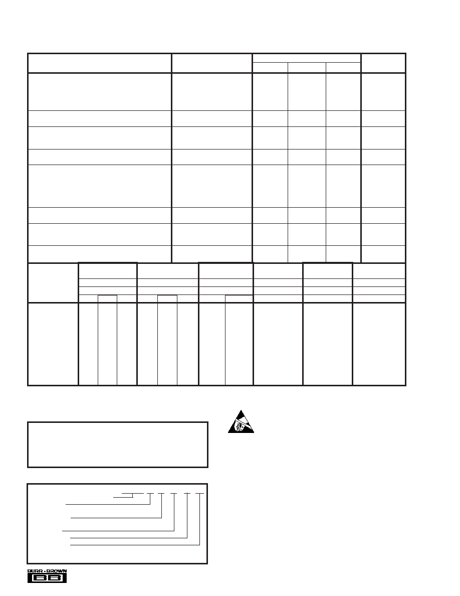
DCP010505B
4.5
5
5.5
4.75
5
5.25
19
31
20
80
3.6
DCP010505DB
4.5
5
5.5
±4.25
±5
±5.75
18
32
22
81
3.8
DCP010512B
4.5
5
5.5
11.4
12
12.6
21
38
29
85
5.1
DCP010512DB
4.5
5
5.5
±11.4
±12
±12.6
19
37
40
82
4.0
DCP010515B
4.5
5
5.5
14.25
15
15.75
26
42
34
82
3.8
DCP010515DB
4.5
5
5.5
±14.25
±15
±15.75
19
41
42
85
4.7
DCP011512DB
13.5
15
16.5
±11.4
±12
±12.6
11
39
19
78
2.5
DCP011515DB
13.5
15
16.5
±14.25
±15
±15.75
12
39
20
80
2.5
DCP012415DB
21.6
24
26.4
±14.25
±15
±15.75
10
35
17
76
3.8
DCP012405B
21.6
24
26.4
4.75
5
5.25
13
23
14
77
2.5
NOTES: (1) During UL1950 recognition tests only. (2) 100% Load Current = 1W/VNOM TYP. (3) Load regulation = (VOUT at 10% Load – VOUT at 100% Load)/VOUT
at 75% Load.
SPECIFICATIONS
At TA = +25°C, unless otherwise specified.
DCP01B SERIES
PARAMETER
CONDITIONS
MIN
TYP
MAX
UNITS
OUTPUT
Power
100% Full Load
0.97
W
Ripple
O/P Capacitor = 1
F, 50% Load
20
mVp-p
Voltage vs Temp
Room to Cold
0.046
%/
°C
Room to Hot
0.016
%/
°C
INPUT
Voltage Range on VS
–10
10
%
ISOLATION
Voltage
1s Flash Test
1
kVrms
60s Test, UL1950(1)
1kVrms
LINE
Regulation
1
%/1% of VS
SWITCHING/SYNCHRONIZATION
Oscillator Frequency (fOSC)
Switching Frequency = fOSC/2
800
kHz
Sync Input Low
0
0.4
V
Sync Input Current
VSYNC = +2V
75
A
Disable Time
2
s
Capacitance Loading on SYNCIN Pin
External
3
pF
RELIABILITY
Demonstrated
TA = +55°C
75
FITS
THERMAL SHUTDOWN
IC Temperature at Shutdown
150
°C
Shutdown Current
3mA
TEMPERATURE RANGE
Operating
–40
+100
°C
DCP01
( B )
相關(guān)PDF資料 |
PDF描述 |
|---|---|
| DCP011512DBP-U/700 | 2-OUTPUT 1 W DC-DC UNREG PWR SUPPLY MODULE |
| DCV010515DP | 2-OUTPUT 1 W DC-DC UNREG PWR SUPPLY MODULE |
| DD15M10GE0 | 15 CONTACT(S), MALE, D SUBMINIATURE CONNECTOR, CRIMP |
| DD36W4P300A00 | 36 CONTACT(S), MALE, D SUBMINIATURE CONNECTOR, SOLDER |
| DDE-1200 | 198 CONTACT(S), FEMALE, SINGLE PART CARD EDGE CONN, WIRE WRAP |
相關(guān)代理商/技術(shù)參數(shù) |
參數(shù)描述 |
|---|---|
| DCP010515DP | 制造商:Texas Instruments 功能描述: |
| DCP010515DP-U | 制造商:BB 制造商全稱:BB 功能描述:Miniature 5V Input, 1W Isolated UNREGULATED DC/DC CONVERTERS |
| DCP010515DP-U/700 | 制造商:BB 制造商全稱:BB 功能描述:Miniature 5V Input, 1W Isolated UNREGULATED DC/DC CONVERTERS |
| DCP010515P | 制造商:BB 制造商全稱:BB 功能描述:Miniature 5V Input, 1W Isolated UNREGULATED DC/DC CONVERTERS |
| DCP010515P-U | 制造商:Rochester Electronics LLC 功能描述:- Bulk |
發(fā)布緊急采購,3分鐘左右您將得到回復。