- 您現在的位置:買賣IC網 > PDF目錄376556 > DAC250Y Dual, 12-Bit, 125MSPS DIGITAL-TO-ANALOG CONVERTER PDF資料下載
參數資料
| 型號: | DAC250Y |
| 英文描述: | Dual, 12-Bit, 125MSPS DIGITAL-TO-ANALOG CONVERTER |
| 中文描述: | 雙通道,12位,125Msps數字模擬轉換器 |
| 文件頁數: | 10/17頁 |
| 文件大小: | 389K |
| 代理商: | DAC250Y |
DAC2902
SBAS167A
10
The value of the load resistance is limited by the output
compliance specification of the DAC2902. To maintain
specified linearity performance, the voltage for I
OUT
and
I
OUT
should not exceed the maximum allowable compliance
range.
The two single-ended output voltages can be combined to
find the total differential output swing:
V
OUTDIFF
=
V
OUT
–
V
OUT
=
(2
Code
–
4095
4096
I
OUTFS
R
LOAD
(7)
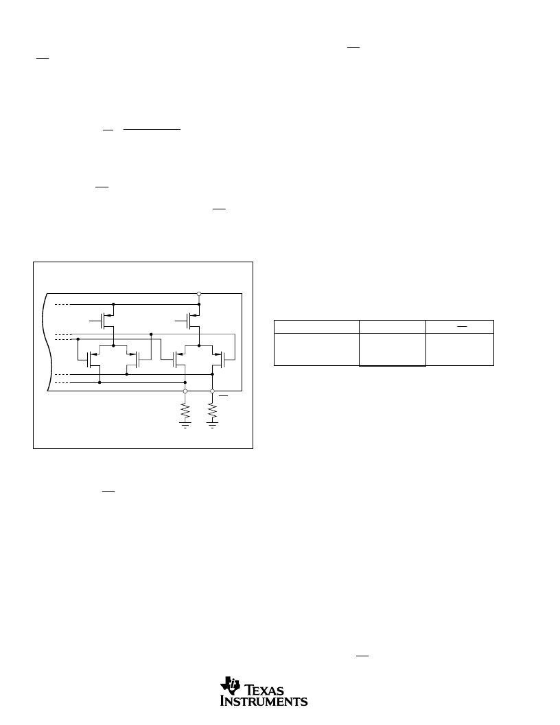
ANALOG OUTPUTS
The DAC2902 provides two complementary current out-
puts, I
OUT
and I
OUT
. The simplified circuit of the analog
output stage representing the differential topology is shown
in Figure 2. The output impedance of I
OUT
and I
OUT
results
from the parallel combination of the differential switches,
along with the current sources and associated parasitic
capacitances.
be adapted to the output of the DAC2902 by selecting a
suitable transformer while maintaining optimum voltage
levels at I
OUT
and I
OUT
. Furthermore, using the differential
output configuration in combination with a transformer will
be instrumental for achieving excellent distortion perfor-
mance. Common-mode errors, such as even-order harmon-
ics or noise, can be substantially reduced. This is particularly
the case with high output frequencies.
For those applications requiring the optimum distortion and
noise performance, it is recommended to select a full-scale
output of 20mA. A lower full-scale range down to 2mA may
be considered for applications that require a low power
consumption, but can tolerate a slightly reduced perfor-
mance level.
OUTPUT CONFIGURATIONS
The current outputs of the DAC2902 allow for a variety of
configurations, some of which are illustrated in Table I. As
mentioned previously, utilizing the converter
’
s differential
outputs will yield the best dynamic performance. Such a
differential output circuit may consist of an RF transformer
or a differential amplifier configuration. The transformer
configuration is ideal for most applications with ac coupling,
while op amps will be suitable for a DC-coupled configura-
tion.
The signal voltage swing that may develop at the two
outputs, I
OUT
and I
OUT
, is limited by a negative and positive
compliance. The negative limit of
–
1V is given by the
breakdown voltage of the CMOS process, and exceeding it
will compromise the reliability of the DAC2902, or even
cause permanent damage. With the full-scale output set to
20mA, the positive compliance equals 1.25V, operating with
an analog supply of +V
A
= 5V. Note that the compliance
range decreases to about 1V for a selected output current of
I
OUTFS
= 2mA. Care should be taken that the configuration
of DAC2902 does not exceed the compliance range to avoid
degradation of the distortion performance and integral lin-
earity.
Best distortion performance is typically achieved with the
maximum full-scale output signal limited to approximately
0.5Vp-p. This is the case for a 50
doubly-terminated load
and a 20mA full-scale output current. A variety of loads can
The single-ended configuration may be considered for appli-
cations requiring a unipolar output voltage. Connecting a
resistor from either one of the outputs to ground will convert
the output current into a ground-referenced voltage signal.
To improve on the DC linearity by maintaining a virtual
ground, an I-to-V or op-amp configuration may be consid-
ered.
DIFFERENTIAL WITH TRANSFORMER
Using an RF transformer provides a convenient way of convert-
ing the differential output signal into a single-ended signal
while achieving excellent dynamic performance (see Figure 3).
The appropriate transformer should be carefully selected based
on the output frequency spectrum and impedance requirements.
The differential transformer configuration has the benefit of
significantly reducing common-mode signals, thus improving
the dynamic performance over a wide range of frequencies.
Furthermore, by selecting a suitable impedance ratio (winding
ratio), the transformer can be used to provide optimum imped-
ance matching while controlling the compliance voltage for the
converter outputs. The model shown, ADTT1-1 (by Mini-
Circuits), has a 1:1 ratio and may be used to interface the
DAC2902 to a 50
load. This results in a 25
load for each of
the outputs, I
OUT
and I
OUT
. The output signals are ac coupled
and inherently isolated because of its magnetic coupling.
FIGURE 2. Equivalent Analog Output.
I
OUT
I
OUT
DAC2902
R
L
R
L
+V
A
INPUT CODE (D11 - D0)
I
OUT
20mA
10mA
0mA
I
OUT
0mA
10mA
20mA
1111 1111 1111
1000 0000 0000
0000 0000 0000
TABLE I. Input Coding Versus Analog Output Current.
相關PDF資料 |
PDF描述 |
|---|---|
| DAC2902Y | Dual, 12-Bit, 125MSPS DIGITAL-TO-ANALOG CONVERTER |
| DAC2KY | Dual, 12-Bit, 125MSPS DIGITAL-TO-ANALOG CONVERTER |
| DAC2902 | Dual, 12-Bit, 125MSPS DIGITAL-TO-ANALOG CONVERTER |
| DAC2902-EVM | Dual, 12-Bit, 125MSPS DIGITAL-TO-ANALOG CONVERTER |
| DAC2900-EVM | DAC2900 10-bit, 125MSPS DC EVM(DAC2900 10位, 125MSPS DC 評估板) |
相關代理商/技術參數 |
參數描述 |
|---|---|
| DAC2534-1 | 制造商:未知廠家 制造商全稱:未知廠家 功能描述:Analog IC |
| DAC2534-2 | 制造商:未知廠家 制造商全稱:未知廠家 功能描述:Analog IC |
| DAC259K59B WAF | 制造商:ON Semiconductor 功能描述: |
| DAC2800D | 制造商:MSK 制造商全稱:M.S. Kennedy Corporation 功能描述:6W DUAL DC - DC CONVERTERS |
| DAC2800S | 制造商:MSK 制造商全稱:M.S. Kennedy Corporation 功能描述:5.4W DC-DC CONVERTERS |
發(fā)布緊急采購,3分鐘左右您將得到回復。