- 您現(xiàn)在的位置:買賣IC網(wǎng) > PDF目錄379101 > CYW15G0403DXB-BGXI (CYPRESS SEMICONDUCTOR CORP) Independent Clock Quad HOTLink II⑩ Transceiver PDF資料下載
參數(shù)資料
| 型號(hào): | CYW15G0403DXB-BGXI |
| 廠商: | CYPRESS SEMICONDUCTOR CORP |
| 元件分類: | 通信及網(wǎng)絡(luò) |
| 英文描述: | Independent Clock Quad HOTLink II⑩ Transceiver |
| 中文描述: | SPECIALTY TELECOM CIRCUIT, PBGA256 |
| 封裝: | 27 X 27 MM, 1.57 MM HEIGHT, LEAD FREE, BGA-256 |
| 文件頁數(shù): | 28/45頁 |
| 文件大小: | 517K |
| 代理商: | CYW15G0403DXB-BGXI |
第1頁第2頁第3頁第4頁第5頁第6頁第7頁第8頁第9頁第10頁第11頁第12頁第13頁第14頁第15頁第16頁第17頁第18頁第19頁第20頁第21頁第22頁第23頁第24頁第25頁第26頁第27頁當(dāng)前第28頁第29頁第30頁第31頁第32頁第33頁第34頁第35頁第36頁第37頁第38頁第39頁第40頁第41頁第42頁第43頁第44頁第45頁
CYP15G0403DXB
CYV15G0403DXB
CYW15G0403DXB
Document #: 38-02065 Rev. *F
Page 28 of 45
Differential CML Serial Outputs: OUTA1
±
, OUTA2
±
, OUTB1
±
, OUTB2
±,
OUTC1
±
, OUTC2
±
, OUTD1
±
, OUTD2
±
V
OHC
Output HIGH Voltage
(V
cc
Referenced)
100
Ω
differential load
150
Ω
differential load
100
Ω
differential load
150
Ω
differential load
100
Ω
differential load
150
Ω
differential load
V
CC
– 0.5
V
CC
– 0.5
V
CC
– 1.4
V
CC
– 1.4
450
560
V
CC
– 0.2
V
CC
– 0.2
V
CC
– 0.7
V
CC
– 0.7
900
1000
V
V
V
V
V
OLC
Output LOW Voltage
(V
CC
Referenced)
V
ODIF
Output Differential Voltage
|(OUT+)
(OUT
)|
mV
mV
Differential Serial Line Receiver Inputs: INA1
±
, INA2
±
, INB1
±
, INB2
±
, INC1
±
, INC2
±
, IND1
±
, IND2
±
V
DIFFs[11]
Input Differential Voltage |(IN+)
(IN
)|
V
IHE
Highest Input HIGH Voltage
V
ILE
Lowest Input LOW Voltage
I
IHE
Input HIGH Current
I
ILE
Input LOW Current
VI
COM[13]
Common Mode input range
100
1200
V
CC
mV
V
V
μ
A
μ
A
V
V
CC
– 2.0
V
IN
= V
IHE
Max.
V
IN
= V
ILE
Min.
((V
CC
– 2.0V)+0.5)min,
(V
CC
– 0.5V) max.
1350
–700
+1.25
+3.1
Power Supply
I
CC [14, 15]
Typ.
910
Max.
1270
1320
1270
1320
Max Power Supply Current
REFCLKx =
MAX
Commercial
Industrial
Commercial
Industrial
mA
mA
mA
mA
I
CC [14, 15]
Typical Power Supply Current
REFCLKx =
125 MHz
900
CYP(V)(W)15G0403DXB DC Electrical Characteristics
(continued)
Parameter
Description
Test Conditions
Min.
Max.
Unit
Notes
13.The common mode range defines the allowable range of INPUT+ and INPUT
when INPUT+ = INPUT
. This marks the zero-crossing between the true and
complement inputs as the signal switches between a logic-1 and a logic-0.
14.Maximum I
is measured with V
CC
= MAX, RFENx = 0, T
A
= 25°C, with all channels and Serial Line Drivers enabled, sending a continuous alternating 01
pattern, and outputs unloaded.
15.Typical I
is measured under similar conditions except with V
= 3.3V, T
= 25°C, RFENx = 0, with all channels enabled and one Serial Line Driver per transmit
channel sending a continuous alternating 01 pattern. The redundant outputs on each channel are powered down and the parallel outputs are unloaded.
16.Cypress uses constant current (ATE) load configurations and forcing functions. This figure is for reference only.
17.The LVTTL switching threshold is 1.4V. All timing references are made relative to where the signal edges cross the threshold voltage.
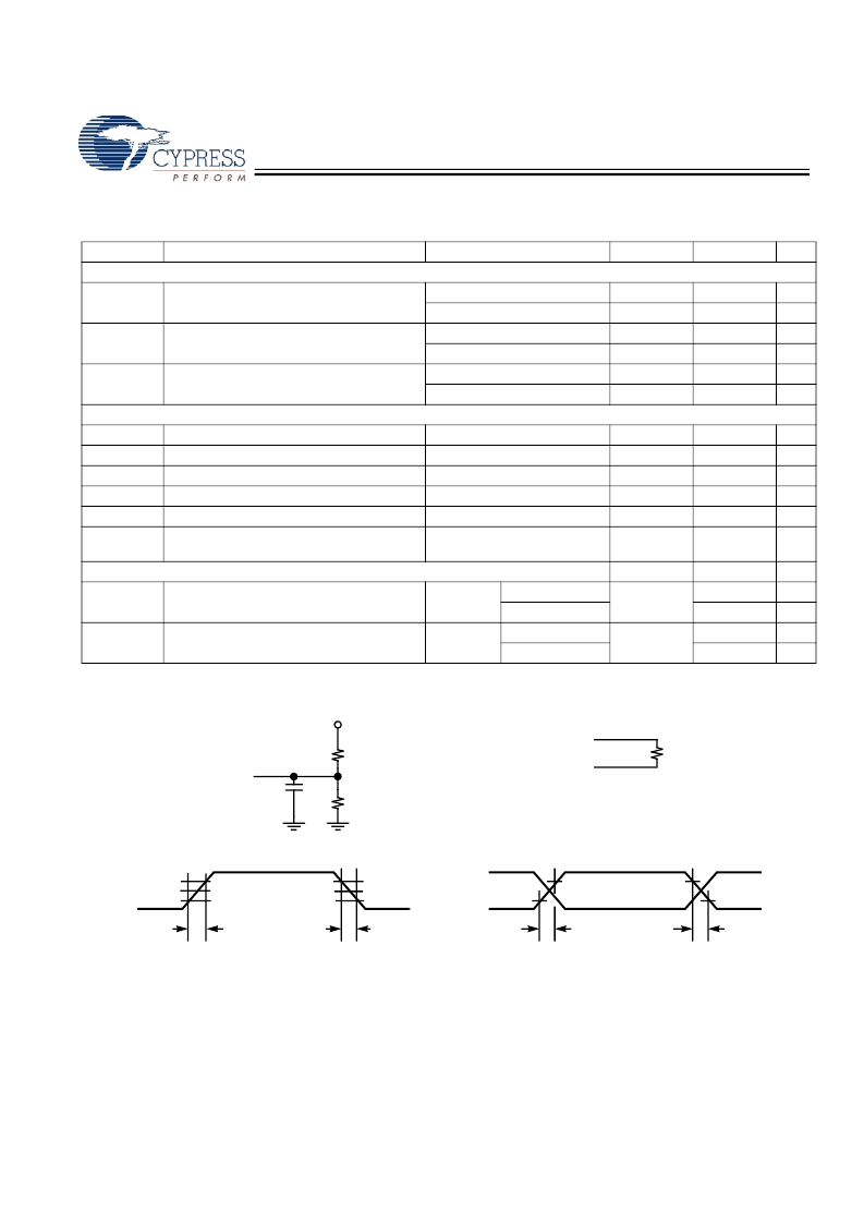
AC Test Loads and Waveforms
2.0V
0.8V
GND
2.0V
0.8V
80%
20%
80%
20%
R
L
(Includes fixture and
probe capacitance)
3.0V
V
th
= 1.4V
≤
270 ps
≤
270 ps
[17]
V
th
= 1.4V
3.3V
R1
R2
R1 = 590
Ω
R2 = 435
Ω
C
L
≤
7 pF
(Includes fixture and
probe capacitance)
(a) LVTTL Output Test Load
R
L
= 100
Ω
(b) CML Output Test Load
C
L
(c) LVTTL Input Test Waveform
(d) CML/LVPECL Input Test Waveform
≤
1 ns
≤
1 ns
V
IHE
V
ILE
V
IHE
V
ILE
[16]
[16]
[+] Feedback
相關(guān)PDF資料 |
PDF描述 |
|---|---|
| CYP15G0403DXB-BGI | Independent Clock Quad HOTLink II⑩ Transceiver |
| CYP15G0403DXB-BGXC | Independent Clock Quad HOTLink II⑩ Transceiver |
| CYP15G0403DXB-BGXI | Independent Clock Quad HOTLink II⑩ Transceiver |
| CYV15G0403DXB-BGC | Independent Clock Quad HOTLink II⑩ Transceiver |
| CYV15G0403DXB-BGI | Independent Clock Quad HOTLink II⑩ Transceiver |
相關(guān)代理商/技術(shù)參數(shù) |
參數(shù)描述 |
|---|---|
| CYW15GO403DXB-BGI | 制造商:Cypress Semiconductor 功能描述: |
| CYW170-01SXC | 功能描述:時(shí)鐘緩沖器 133MHz Clock RoHS:否 制造商:Texas Instruments 輸出端數(shù)量:5 最大輸入頻率:40 MHz 傳播延遲(最大值): 電源電壓-最大:3.45 V 電源電壓-最小:2.375 V 最大功率耗散: 最大工作溫度:+ 85 C 最小工作溫度:- 40 C 封裝 / 箱體:LLP-24 封裝:Reel |
| CYW170-01SXCT | 功能描述:時(shí)鐘緩沖器 133MHz Clock RoHS:否 制造商:Texas Instruments 輸出端數(shù)量:5 最大輸入頻率:40 MHz 傳播延遲(最大值): 電源電壓-最大:3.45 V 電源電壓-最小:2.375 V 最大功率耗散: 最大工作溫度:+ 85 C 最小工作溫度:- 40 C 封裝 / 箱體:LLP-24 封裝:Reel |
| CYW173SXC | 功能描述:時(shí)鐘發(fā)生器及支持產(chǎn)品 Tape Media Backup Dr Clk Gen W173 DS RoHS:否 制造商:Silicon Labs 類型:Clock Generators 最大輸入頻率:14.318 MHz 最大輸出頻率:166 MHz 輸出端數(shù)量:16 占空比 - 最大:55 % 工作電源電壓:3.3 V 工作電源電流:1 mA 最大工作溫度:+ 85 C 安裝風(fēng)格:SMD/SMT 封裝 / 箱體:QFN-56 |
| CYW173SXCT | 功能描述:時(shí)鐘發(fā)生器及支持產(chǎn)品 Tape Media Backup Dr Clk Gen W173 DS RoHS:否 制造商:Silicon Labs 類型:Clock Generators 最大輸入頻率:14.318 MHz 最大輸出頻率:166 MHz 輸出端數(shù)量:16 占空比 - 最大:55 % 工作電源電壓:3.3 V 工作電源電流:1 mA 最大工作溫度:+ 85 C 安裝風(fēng)格:SMD/SMT 封裝 / 箱體:QFN-56 |
發(fā)布緊急采購,3分鐘左右您將得到回復(fù)。