- 您現(xiàn)在的位置:買賣IC網 > PDF目錄378516 > CYM9271B (Cypress Semiconductor Corp.) 128K x 36 SRAM Module(128K x 36 靜態(tài)RAM模塊) PDF資料下載
參數(shù)資料
| 型號: | CYM9271B |
| 廠商: | Cypress Semiconductor Corp. |
| 英文描述: | 128K x 36 SRAM Module(128K x 36 靜態(tài)RAM模塊) |
| 中文描述: | 128K的× 36的SRAM模塊(128K的× 36靜態(tài)內存模塊) |
| 文件頁數(shù): | 6/10頁 |
| 文件大?。?/td> | 149K |
| 代理商: | CYM9271B |
CYM9270
CYM9271B
CYM9272A
CYM9273
6
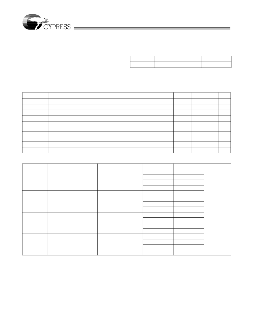
Maximum Ratings
(Above which the useful life may be impaired. For user guide-
lines, not tested.)
Storage Temperature .................................
–
55
°
C to +125
°
C
Ambient Temperature
with Power Applied.........................................
–
0
°
C to +70
°
C
3.3V Supply Voltage to Ground Potential......
–
0.5V to +4.5V
DC Voltage Applied to Outputs
in High Z State..............................................
–
0.5V to +4.6V
DC Input Voltage ...........................................
–
0.5V to +4.6V
Output Current into Outputs (LOW)............................. 20 mA
Operating Range
Range
Commercial
AmbientTemperature
0
°
C to +70
°
C
V
CC
3.3V
±
5%
Electrical Characteristics
Over the Operating Range
Parameter
V
IH
V
IL
V
OH
V
OL
I
CC (9270)
Description
Test Condition
Min.
2.2
–
0.3
2.4
Max.
Unit
V
V
V
V
mA
Input HIGH Voltage
Input LOW Voltage
Output HIGH Voltage
Output LOW Voltage
V
CC
Operating Supply Current
V
CC
+ 0.3
0.8
V
CC
=Min. I
OH
=
4 mA
V
CC
=Min. I
OL
= 8 mA
V
CC
=Max., I
OUT
=0 mA, f=f
MAX
=1/t
RC
0.4
350
I
CC (9271B)
V
CC
Operating Supply Current
V
CC
=Max., I
OUT
=0 mA, f=f
MAX
=1/t
RC
500
mA
I
CC (9272A)
I
CC (9273)
V
CC
Operating Supply Current
V
CC
Operating Supply Current
V
CC
=Max., I
OUT
=0 mA, f=f
MAX
=1/t
RC
V
CC
=Max., I
OUT
=0 mA, f=f
MAX
=1/t
RC
1000
1200
mA
mA
Capacitance
[1]
Parameter
C
A
Description
Test Conditions
T
A
= 25
°
C, f = 1 MHz,
V
CC
= 5.0V
Max.
9270
9271B
9272A
9273
9270
9271B
9272A
9273
9270
9271B
9272A
9273
9270
9271B
9272A
9273
Max.
12
7
14
20
12
8
16
20
9
5
10
16
6
3
3
5
Unit
pF
Address Input Capacitance
C
I
Control Input Capacitance
T
A
= 25
°
C, f = 1 MHz,
V
CC
= 5.0V
C
O
Input / Output Capacitance
T
A
= 25
°
C, f = 1 MHz,
V
CC
= 5.0V
C
CLK
Clock Capacitance
T
A
= 25
°
C, f = 1 MHz,
V
CC
= 5.0V
Note:
1.
Tested initially and after any design or process changes that may affect these parameters.
相關PDF資料 |
PDF描述 |
|---|---|
| CYM9270 | 64K x 36 SRAM Module(64K x 36 靜態(tài)RAM模塊) |
| CYM9272A | 256K x 36 SRAM Module(256K x 36 靜態(tài)RAM模塊) |
| CYM9273 | 512K x 36 SRAM Module(512K x 36 靜態(tài)RAM模塊) |
| CYN17-4 | Connector assemblies, Audio/RF/Video cables; |
| CYP15G0401DXA | Quad HOTLink II Transceiver |
相關代理商/技術參數(shù) |
參數(shù)描述 |
|---|---|
| CYM9271CPM-50C | 制造商:MAJOR 功能描述: |
| CYM9273 | 制造商:未知廠家 制造商全稱:未知廠家 功能描述:Memory |
| CYM9273PM-50C | 制造商:未知廠家 制造商全稱:未知廠家 功能描述:x36 Synchronous SRAM Module |
| CYM9275PM-100C | 制造商:未知廠家 制造商全稱:未知廠家 功能描述:x36 Synchronous SRAM Module |
| CYM9275PM-133C | 制造商:未知廠家 制造商全稱:未知廠家 功能描述:x36 Synchronous SRAM Module |
發(fā)布緊急采購,3分鐘左右您將得到回復。