- 您現(xiàn)在的位置:買賣IC網(wǎng) > PDF目錄378516 > CY8C29566 (Cypress Semiconductor Corp.) RES. 0603, SMD, 0.1%, TNF, 25PPM/C 100 OHM PDF資料下載
參數(shù)資料
| 型號: | CY8C29566 |
| 廠商: | Cypress Semiconductor Corp. |
| 英文描述: | RES. 0603, SMD, 0.1%, TNF, 25PPM/C 100 OHM |
| 中文描述: | 混合信號陣列 |
| 文件頁數(shù): | 8/40頁 |
| 文件大小: | 474K |
| 代理商: | CY8C29566 |
第1頁第2頁第3頁第4頁第5頁第6頁第7頁當(dāng)前第8頁第9頁第10頁第11頁第12頁第13頁第14頁第15頁第16頁第17頁第18頁第19頁第20頁第21頁第22頁第23頁第24頁第25頁第26頁第27頁第28頁第29頁第30頁第31頁第32頁第33頁第34頁第35頁第36頁第37頁第38頁第39頁第40頁
August 3, 2004
Document No. 38-12013 Rev. *F
8
1.
Pin Information
This chapter describes, lists, and illustrates the CY8C29x66 PSoC device pins and pinout configurations.
1.1
Pinouts
The CY8C29x66 PSoC device is available in a variety of packages which are listed and illustrated in the following tables. Every port
pin (labeled with a “P”) is capable of Digital IO. However, Vss, Vdd, SMP, and XRES are not capable of Digital IO.
1.1.1
28-Pin Part Pinout
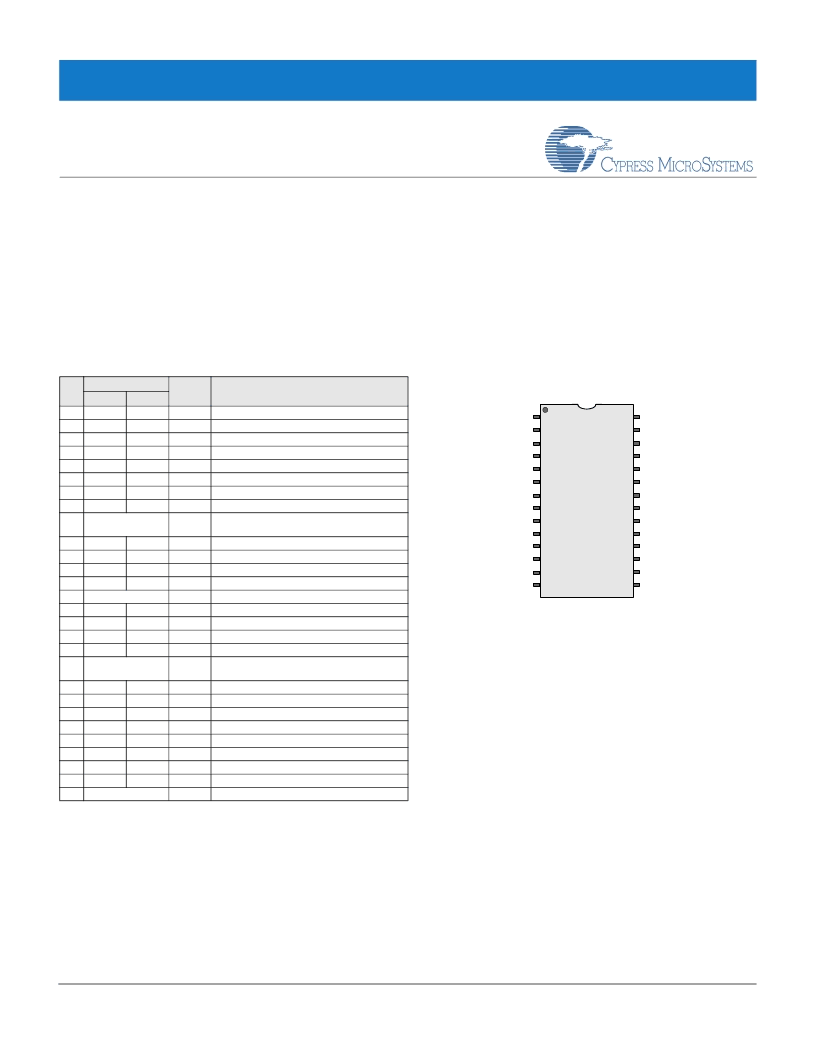
Table 1-1. 28-Pin Part Pinout (PDIP, SSOP, SOIC)
Pin
No.
1
2
3
4
5
6
7
8
9
Type
Pin
Name
P0[7]
P0[5]
P0[3]
P0[1]
P2[7]
P2[5]
P2[3]
P2[1]
SMP
Description
CY8C29466 28-Pin PSoC Device
Digital
IO
IO
IO
IO
IO
IO
IO
IO
Analog
I
IO
IO
I
Analog column mux input.
Analog column mux input and column output.
Analog column mux input and column output.
Analog column mux input.
I
I
Direct switched capacitor block input.
Direct switched capacitor block input.
Switch Mode Pump (SMP) connection to
external components required.
I2C Serial Clock (SCL)
I2C Serial Data (SDA)
Power
10
11
12
13
14
15
16
17
18
19
IO
IO
IO
IO
P1[7]
P1[5]
P1[3]
P1[1]
Vss
P1[0]
P1[2]
P1[4]
P1[6]
XRES
Crystal (XTALin), I2C Serial Clock (SCL)
Ground connection.
Crystal (XTALout), I2C Serial Data (SDA)
Power
IO
IO
IO
IO
Optional External Clock Input (EXTCLK)
Input
Active high external reset with internal pull
down.
Direct switched capacitor block input.
Direct switched capacitor block input.
External Analog Ground (AGND)
External Voltage Reference (VREF)
Analog column mux input.
Analog column mux input and column output.
Analog column mux input and column output.
Analog column mux input.
Supply voltage.
20
21
22
23
24
25
26
27
28
IO
IO
IO
IO
IO
IO
IO
IO
I
I
P2[0]
P2[2]
P2[4]
P2[6]
P0[0]
P0[2]
P0[4]
P0[6]
Vdd
I
IO
IO
I
Power
LEGEND
: A = Analog, I = Input, and O = Output.
AI, P0[7]
AIO, P0[5]
AIO, P0[3]
AI, P0[1]
P2[7]
P2[5]
AI, P2[3]
AI, P2[1]
SMP
I2C SCL, P1[7]
I2C SDA, P1[5]
P1[3]
I2C SCL, XTALin, P1[1]
Vss
Vdd
P0[6], AI
P0[4], AIO
P0[2], AIO
P0[0], AI
P2[6], External VREF
P2[4], External AGND
P2[2], AI
P2[0], AI
XRES
P1[6]
P1[4], EXTCLK
P1[2]
P1[0], XTALout, I2C SDA
PDIP
SSOP
SOIC
1
2
3
4
5
6
7
8
9
10
11
12
13
14
28
27
26
25
24
23
22
21
20
19
18
17
16
15
相關(guān)PDF資料 |
PDF描述 |
|---|---|
| CY8C29666 | Mixed Signal Array |
| CY8C29666-24PVXI | Mixed Signal Array |
| CY8C29866 | Mixed Signal Array |
| CY8C29466-24PXI | Mixed Signal Array |
| CY8C29566-24AXI | Mixed Signal Array |
相關(guān)代理商/技術(shù)參數(shù) |
參數(shù)描述 |
|---|---|
| CY8C29566-24AXI | 功能描述:可編程片上系統(tǒng) - PSoC IC MCU 32K FLASH 2K SRAM RoHS:否 制造商:Cypress Semiconductor 核心:8051 處理器系列:CY8C36 數(shù)據(jù)總線寬度:8 bit 最大時鐘頻率:67 MHz 程序存儲器大小:32 KB 數(shù)據(jù) RAM 大小:4 KB 片上 ADC:Yes 工作電源電壓:0.5 V to 5.5 V 工作溫度范圍:- 40 C to + 85 C 封裝 / 箱體:QFN-68 安裝風(fēng)格:SMD/SMT |
| CY8C29566-24AXIT | 功能描述:可編程片上系統(tǒng) - PSoC 32K Flsh 2KB RAM IND RoHS:否 制造商:Cypress Semiconductor 核心:8051 處理器系列:CY8C36 數(shù)據(jù)總線寬度:8 bit 最大時鐘頻率:67 MHz 程序存儲器大小:32 KB 數(shù)據(jù) RAM 大小:4 KB 片上 ADC:Yes 工作電源電壓:0.5 V to 5.5 V 工作溫度范圍:- 40 C to + 85 C 封裝 / 箱體:QFN-68 安裝風(fēng)格:SMD/SMT |
| CY8C2966-12PVXE | 制造商:Cypress Semiconductor 功能描述: |
| CY8C29666-12PVXE | 功能描述:可編程片上系統(tǒng) - PSoC 44 I/O 32K Flash 2K bytes RAM RoHS:否 制造商:Cypress Semiconductor 核心:8051 處理器系列:CY8C36 數(shù)據(jù)總線寬度:8 bit 最大時鐘頻率:67 MHz 程序存儲器大小:32 KB 數(shù)據(jù) RAM 大小:4 KB 片上 ADC:Yes 工作電源電壓:0.5 V to 5.5 V 工作溫度范圍:- 40 C to + 85 C 封裝 / 箱體:QFN-68 安裝風(fēng)格:SMD/SMT |
| CY8C29666-12PVXET | 功能描述:可編程片上系統(tǒng) - PSoC 44 I/O 32K Flash 2K bytes RAM RoHS:否 制造商:Cypress Semiconductor 核心:8051 處理器系列:CY8C36 數(shù)據(jù)總線寬度:8 bit 最大時鐘頻率:67 MHz 程序存儲器大小:32 KB 數(shù)據(jù) RAM 大小:4 KB 片上 ADC:Yes 工作電源電壓:0.5 V to 5.5 V 工作溫度范圍:- 40 C to + 85 C 封裝 / 箱體:QFN-68 安裝風(fēng)格:SMD/SMT |
發(fā)布緊急采購,3分鐘左右您將得到回復(fù)。