- 您現(xiàn)在的位置:買賣IC網(wǎng) > PDF目錄378516 > CY8C29466-24SXI (CYPRESS SEMICONDUCTOR CORP) Mixed Signal Array PDF資料下載
參數(shù)資料
| 型號(hào): | CY8C29466-24SXI |
| 廠商: | CYPRESS SEMICONDUCTOR CORP |
| 元件分類: | 外設(shè)及接口 |
| 英文描述: | Mixed Signal Array |
| 中文描述: | MULTIFUNCTION PERIPHERAL, PDSO28 |
| 封裝: | 0.300 INCH, LEAD FREE, MO-119, SOIC-28 |
| 文件頁數(shù): | 23/40頁 |
| 文件大小: | 474K |
| 代理商: | CY8C29466-24SXI |
第1頁第2頁第3頁第4頁第5頁第6頁第7頁第8頁第9頁第10頁第11頁第12頁第13頁第14頁第15頁第16頁第17頁第18頁第19頁第20頁第21頁第22頁當(dāng)前第23頁第24頁第25頁第26頁第27頁第28頁第29頁第30頁第31頁第32頁第33頁第34頁第35頁第36頁第37頁第38頁第39頁第40頁
August 3, 2004
Document No. 38-12013 Rev. *F
23
CY8C29x66 Preliminary Data Sheet
3. Electrical Specifications
3.3.6
DC Analog Reference Specifications
The following tables list guaranteed maximum and minimum specifications for the voltage and temperature ranges: 4.75V to 5.25V
and -40
°
C
≤
T
A
≤
85
°
C, or 3.0V to 3.6V and -40
°
C
≤
T
A
≤
85
°
C, respectively. Typical parameters apply to 5V and 3.3V at 25
°
C and
are for design guidance only.
The guaranteed specifications are measured through the Analog Continuous Time PSoC blocks. The power levels for AGND refer to
the power of the Analog Continuous Time PSoC block. The power levels for RefHi and RefLo refer to the Analog Reference Control
register. The limits stated for AGND include the offset error of the AGND buffer local to the Analog Continuous Time PSoC block.
Reference control power is high.
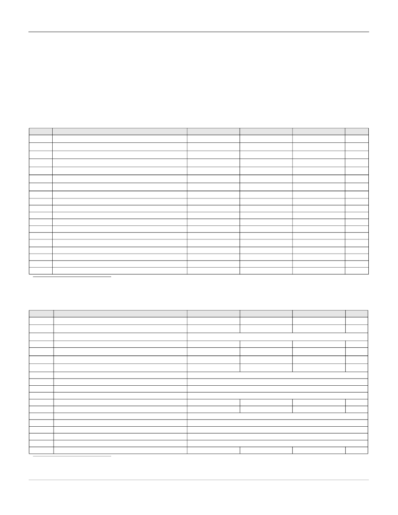
Table 3-11: 5V DC Analog Reference Specifications
Symbol
V
BG5
–
Description
Min
Typ
Max
Units
Bandgap Voltage Reference 5V
1.28
Vdd/2 - 0.02
1.30
Vdd/2
1.32
Vdd/2 + 0.02
V
V
AGND = Vdd/2
a
AGND = 2 x BandGap
a
AGND = P2[4] (P2[4] = Vdd/2)
a
AGND = BandGap
a
AGND = 1.6 x BandGap
a
AGND Block to Block Variation (AGND = Vdd/2)
a
RefHi = Vdd/2 + BandGap
RefHi = 3 x BandGap
RefHi = 2 x BandGap + P2[6] (P2[6] = 1.3V)
RefHi = P2[4] + BandGap (P2[4] = Vdd/2)
RefHi = P2[4] + P2[6] (P2[4] = Vdd/2, P2[6] = 1.3V)
RefHi = 2 x BandGap
RefHi = 3.2 x BandGap
RefLo = Vdd/2 – BandGap
RefLo = BandGap
RefLo = 2 x BandGap - P2[6] (P2[6] = 1.3V)
RefLo = P2[4] – BandGap (P2[4] = Vdd/2)
RefLo = P2[4]-P2[6] (P2[4] = Vdd/2, P2[6] = 1.3V)
a. AGND tolerance includes the offsets of the local buffer in the PSoC block. Bandgap voltage is 1.3V ± 0.02V.
–
2.52
2.60
2.72
V
–
P2[4] - 0.013
P2[4]
P2[4] + 0.013
V
–
1.27
1.3
1.34
V
–
2.03
2.08
2.13
V
–
-0.034
Vdd
/2 + 1.21
3.75
P2[6] + 2.478
P2[4] + 1.218
P2[4] + P2[6] - 0.058
2.50
4.02
Vdd
/2 - 1.369
1.20
2.489 - P2[6]
P2[4] - 1.368
P2[4] - P2[6] - 0.042
0.000
Vdd
/2 + 1.3
3.9
P2[6] + 2.6
P2[4] + 1.3
P2[4] + P2[6]
2.60
4.16
Vdd
/2 - 1.30
1.30
2.6 - P2[6]
P2[4] - 1.30
P2[4] - P2[6]
0.034
Vdd
/2 + 1.382
4.05
P2[6] + 2.722
P2[4] + 1.382
P2[4] + P2[6] + 0.058
2.70
4.29
Vdd
/2 - 1.231
1.40
2.711 - P2[6]
P2[4] - 1.232
P2[4] - P2[6] + 0.042
V
–
–
–
–
–
–
–
–
–
–
–
–
V
V
V
V
V
V
V
V
V
V
V
V
Table 3-12: 3.3V DC Analog Reference Specifications
Symbol
V
BG33
–
Description
Min
Typ
Max
Units
Bandgap Voltage Reference 3.3V
1.28
1.30
1.32
V
AGND = Vdd/2
a
AGND = 2 x BandGap
a
AGND = P2[4] (P2[4] = Vdd/2)
AGND = BandGap
a
AGND = 1.6 x BandGap
a
AGND Block to Block Variation (AGND = Vdd/2)
a
RefHi = Vdd/2 + BandGap
RefHi = 3 x BandGap
RefHi = 2 x BandGap + P2[6] (P2[6] = 0.5V)
RefHi = P2[4] + BandGap (P2[4] = Vdd/2)
RefHi = P2[4] + P2[6] (P2[4] = Vdd/2, P2[6] = 0.5V)
RefHi = 2 x BandGap
RefHi = 3.2 x BandGap
RefLo = Vdd/2 - BandGap
RefLo = BandGap
RefLo = 2 x BandGap - P2[6] (P2[6] = 0.5V)
RefLo = P2[4] – BandGap (P2[4] = Vdd/2)
RefLo = P2[4]-P2[6] (P2[4] = Vdd/2, P2[6] = 0.5V)
a. AGND tolerance includes the offsets of the local buffer in the PSoC block. Bandgap voltage is 1.3V ± 0.02V.
Vdd/2 - 0.02
Vdd/2
Vdd/2 + 0.02
V
–
Not Allowed
P2[4] - 0.009
1.27
–
–
P2[4]
1.30
P2[4] + 0.009
1.34
V
V
–
2.03
2.08
2.13
V
–
-0.034
0.000
0.034
mV
–
–
–
–
–
–
–
–
–
–
–
–
Not Allowed
Not Allowed
Not Allowed
Not Allowed
P2[4] + P2[6] - 0.042
2.50
Not Allowed
Not Allowed
Not Allowed
Not Allowed
Not Allowed
P2[4] - P2[6] - 0.036
P2[4] + P2[6]
2.60
P2[4] + P2[6] + 0.042
2.70
V
V
P2[4] - P2[6]
P2[4] - P2[6] + 0.036
V
相關(guān)PDF資料 |
PDF描述 |
|---|---|
| CY8C29466-24SXIT | Mixed Signal Array |
| CY8C29566 | RES. 0603, SMD, 0.1%, TNF, 25PPM/C 100 OHM |
| CY8C29666 | Mixed Signal Array |
| CY8C29666-24PVXI | Mixed Signal Array |
| CY8C29866 | Mixed Signal Array |
相關(guān)代理商/技術(shù)參數(shù) |
參數(shù)描述 |
|---|---|
| CY8C29466-24SXIT | 功能描述:可編程片上系統(tǒng) - PSoC 32K Flsh 2KB RAM IND RoHS:否 制造商:Cypress Semiconductor 核心:8051 處理器系列:CY8C36 數(shù)據(jù)總線寬度:8 bit 最大時(shí)鐘頻率:67 MHz 程序存儲(chǔ)器大小:32 KB 數(shù)據(jù) RAM 大小:4 KB 片上 ADC:Yes 工作電源電壓:0.5 V to 5.5 V 工作溫度范圍:- 40 C to + 85 C 封裝 / 箱體:QFN-68 安裝風(fēng)格:SMD/SMT |
| CY8C294664-24PVXI | 功能描述:PROGRAMMABLE SYSTEM ON A CHIP RoHS:是 類別:未定義的類別 >> 其它 系列:* 標(biāo)準(zhǔn)包裝:1 系列:* 其它名稱:MS305720A |
| CY8C294665-24PVXI | 制造商:Cypress Semiconductor 功能描述: |
| CY8C29566-24AXI | 功能描述:可編程片上系統(tǒng) - PSoC IC MCU 32K FLASH 2K SRAM RoHS:否 制造商:Cypress Semiconductor 核心:8051 處理器系列:CY8C36 數(shù)據(jù)總線寬度:8 bit 最大時(shí)鐘頻率:67 MHz 程序存儲(chǔ)器大小:32 KB 數(shù)據(jù) RAM 大小:4 KB 片上 ADC:Yes 工作電源電壓:0.5 V to 5.5 V 工作溫度范圍:- 40 C to + 85 C 封裝 / 箱體:QFN-68 安裝風(fēng)格:SMD/SMT |
| CY8C29566-24AXIT | 功能描述:可編程片上系統(tǒng) - PSoC 32K Flsh 2KB RAM IND RoHS:否 制造商:Cypress Semiconductor 核心:8051 處理器系列:CY8C36 數(shù)據(jù)總線寬度:8 bit 最大時(shí)鐘頻率:67 MHz 程序存儲(chǔ)器大小:32 KB 數(shù)據(jù) RAM 大小:4 KB 片上 ADC:Yes 工作電源電壓:0.5 V to 5.5 V 工作溫度范圍:- 40 C to + 85 C 封裝 / 箱體:QFN-68 安裝風(fēng)格:SMD/SMT |
發(fā)布緊急采購,3分鐘左右您將得到回復(fù)。