- 您現(xiàn)在的位置:買(mǎi)賣(mài)IC網(wǎng) > PDF目錄378516 > CY8C27666-SPSXI (Cypress Semiconductor Corp.) PSoC⑩ Mixed Signal Array PDF資料下載
參數(shù)資料
| 型號(hào): | CY8C27666-SPSXI |
| 廠商: | Cypress Semiconductor Corp. |
| 英文描述: | PSoC⑩ Mixed Signal Array |
| 中文描述: | ⑩的PSoC混合信號(hào)陣列 |
| 文件頁(yè)數(shù): | 6/39頁(yè) |
| 文件大?。?/td> | 610K |
| 代理商: | CY8C27666-SPSXI |
第1頁(yè)第2頁(yè)第3頁(yè)第4頁(yè)第5頁(yè)當(dāng)前第6頁(yè)第7頁(yè)第8頁(yè)第9頁(yè)第10頁(yè)第11頁(yè)第12頁(yè)第13頁(yè)第14頁(yè)第15頁(yè)第16頁(yè)第17頁(yè)第18頁(yè)第19頁(yè)第20頁(yè)第21頁(yè)第22頁(yè)第23頁(yè)第24頁(yè)第25頁(yè)第26頁(yè)第27頁(yè)第28頁(yè)第29頁(yè)第30頁(yè)第31頁(yè)第32頁(yè)第33頁(yè)第34頁(yè)第35頁(yè)第36頁(yè)第37頁(yè)第38頁(yè)第39頁(yè)
June 1, 2004
Document No. 38-12019 Rev. *B
6
CY8C27x66 Preliminary Data Sheet
PSoC Overview
User Modules and the PSoC
Development Process
The development process for the PSoC device differs from that
of a traditional fixed function microprocessor. The configurable
analog and digital hardware blocks give the PSoC architecture
a unique flexibility that pays dividends in managing specification
change during development and by lowering inventory costs.
These configurable resources, called PSoC Blocks, have the
ability to implement a wide variety of user-selectable functions.
Each block has several registers that determine its function and
connectivity to other blocks, multiplexers, buses, and to the IO
pins. Iterative development cycles permit you to adapt the hard-
ware as well as the software. This substantially lowers the risk
of having to select a different part to meet the final design
requirements.
To speed the development process, the PSoC Designer Inte-
grated Development Environment (IDE) provides a library of
pre-built, pre-tested hardware peripheral functions, called “User
Modules.” User modules make selecting and implementing
peripheral devices simple, and come in analog, digital, and
mixed signal varieties. The standard User Module library con-
tains over 50 common peripherals such as ADCs, DACs Tim-
ers, Counters, UARTs, and other not-so common peripherals
such as DTMF Generators and Bi-Quad analog filter sections.
Each user module establishes the basic register settings that
implement the selected function. It also provides parameters
that allow you to tailor its precise configuration to your particular
application. For example, a Pulse Width Modulator User Mod-
ule configures one or more digital PSoC blocks, one for each 8
bits of resolution. The user module parameters permit you to
establish the pulse width and duty cycle. User modules also
provide tested software to cut your development time. The user
module application programming interface (API) provides high-
level functions to control and respond to hardware events at
run-time. The API also provides optional interrupt service rou-
tines that you can adapt as needed.
The API functions are documented in user module data sheets
that are viewed directly in the PSoC Designer IDE. These data
sheets explain the internal operation of the user module and
provide performance specifications. Each data sheet describes
the use of each user module parameter and documents the set-
ting of each register controlled by the user module.
The development process starts when you open a new project
and bring up the Device Editor, a pictorial environment (GUI) for
configuring the hardware. You pick the user modules you need
for your project and map them onto the PSoC blocks with point-
and-click simplicity. Next, you build signal chains by intercon-
necting user modules to each other and the IO pins. At this
stage, you also configure the clock source connections and
enter parameter values directly or by selecting values from
drop-down menus. When you are ready to test the hardware
configuration or move on to developing code for the project, you
perform the “Generate Application” step. This causes PSoC
Designer to generate source code that automatically configures
the device to your specification and provides the high-level user
module API functions.
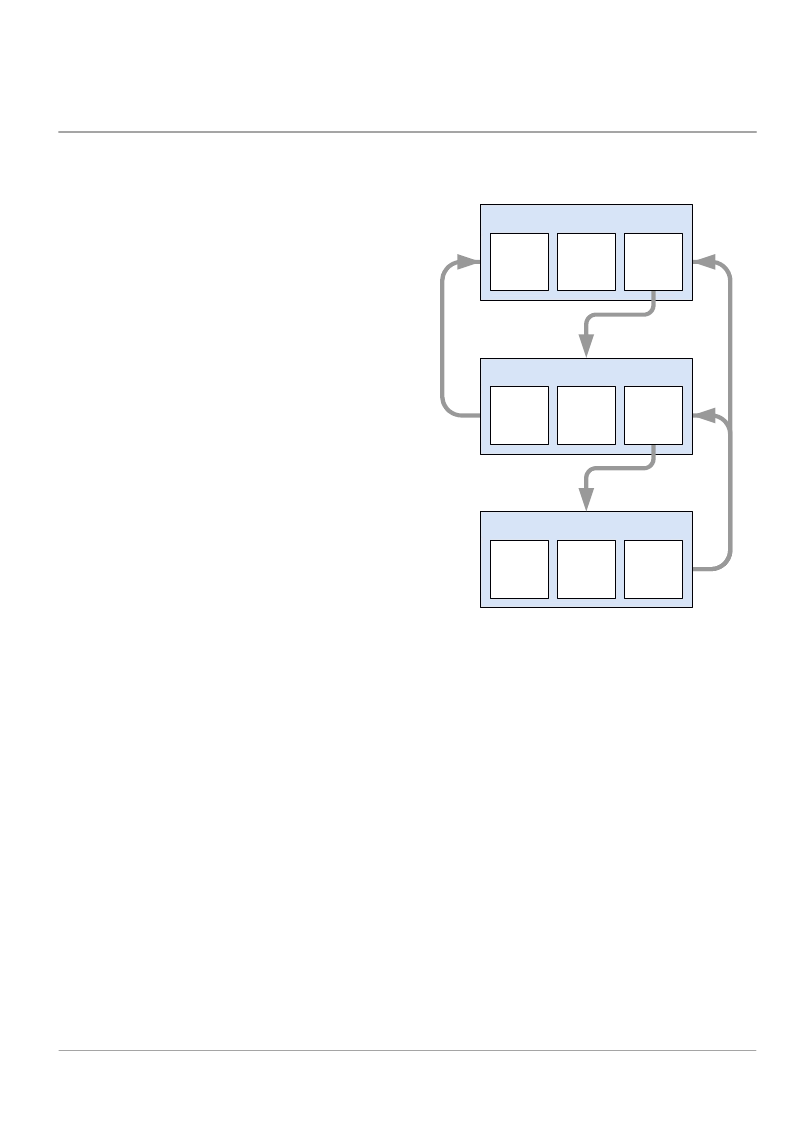
User Module and Source Code Development Flows
The next step is to write your main program, and any sub-rou-
tines using PSoC Designer’s Application Editor subsystem.
The Application Editor includes a Project Manager that allows
you to open the project source code files (including all gener-
ated code files) from a hierarchal view. The source code editor
provides syntax coloring and advanced edit features for both C
and assembly language. File search capabilities include simple
string searches and recursive “grep-style” patterns. A single
mouse click invokes the Build Manager. It employs a profes-
sional-strength “makefile” system to automatically analyze all
file dependencies and run the compiler and assembler as nec-
essary. Project-level options control optimization strategies
used by the compiler and linker. Syntax errors are displayed in
a console window. Double clicking the error message takes you
directly to the offending line of source code. When all is correct,
the linker builds a ROM file image suitable for programming.
The last step in the development process takes place inside the
PSoC Designer’s Debugger subsystem. The Debugger down-
loads the ROM image to the In-Circuit Emulator (ICE) where it
runs at full speed. Debugger capabilities rival those of systems
costing many times more. In addition to traditional single-step,
run-to-breakpoint and watch-variable features, the Debugger
provides a large trace buffer and allows you define complex
breakpoint events that include monitoring address and data bus
values, memory locations and external signals.
Debugger
Interface
to ICE
Application Editor
Device Editor
Project
Manager
Source
Code
Editor
Storage
Inspector
User
Module
Selection
Placement
and
Parameter
-ization
Generate
Application
Build
All
Event &
Breakpoint
Manager
Build
Manager
Source
Code
Generator
相關(guān)PDF資料 |
PDF描述 |
|---|---|
| CY8C29466-24PVXI | Mixed Signal Array |
| CY8C29466-24PVXIT | Mixed Signal Array |
| CY8C29666-24PVXIT | Mixed Signal Array |
| CY8C29666-24LFXI | Mixed Signal Array |
| CY8C29866-24AXI | Mixed Signal Array |
相關(guān)代理商/技術(shù)參數(shù) |
參數(shù)描述 |
|---|---|
| CY8C28000-24PVXI | 制造商:Cypress Semiconductor 功能描述: |
| CY8C28243-24PVXI | 功能描述:可編程片上系統(tǒng) - PSoC PSoC Programmable System-on-Chip RoHS:否 制造商:Cypress Semiconductor 核心:8051 處理器系列:CY8C36 數(shù)據(jù)總線寬度:8 bit 最大時(shí)鐘頻率:67 MHz 程序存儲(chǔ)器大小:32 KB 數(shù)據(jù) RAM 大小:4 KB 片上 ADC:Yes 工作電源電壓:0.5 V to 5.5 V 工作溫度范圍:- 40 C to + 85 C 封裝 / 箱體:QFN-68 安裝風(fēng)格:SMD/SMT |
| CY8C28243-24PVXIT | 功能描述:可編程片上系統(tǒng) - PSoC 16 I/O 16K FLASH 1K SRAM RoHS:否 制造商:Cypress Semiconductor 核心:8051 處理器系列:CY8C36 數(shù)據(jù)總線寬度:8 bit 最大時(shí)鐘頻率:67 MHz 程序存儲(chǔ)器大小:32 KB 數(shù)據(jù) RAM 大小:4 KB 片上 ADC:Yes 工作電源電壓:0.5 V to 5.5 V 工作溫度范圍:- 40 C to + 85 C 封裝 / 箱體:QFN-68 安裝風(fēng)格:SMD/SMT |
| CY8C28403-24PVXI | 功能描述:可編程片上系統(tǒng) - PSoC PSoC Programmable System-on-Chip RoHS:否 制造商:Cypress Semiconductor 核心:8051 處理器系列:CY8C36 數(shù)據(jù)總線寬度:8 bit 最大時(shí)鐘頻率:67 MHz 程序存儲(chǔ)器大小:32 KB 數(shù)據(jù) RAM 大小:4 KB 片上 ADC:Yes 工作電源電壓:0.5 V to 5.5 V 工作溫度范圍:- 40 C to + 85 C 封裝 / 箱體:QFN-68 安裝風(fēng)格:SMD/SMT |
| CY8C28403-24PVXIT | 功能描述:可編程片上系統(tǒng) - PSoC PSoC Programmable System-on-Chip RoHS:否 制造商:Cypress Semiconductor 核心:8051 處理器系列:CY8C36 數(shù)據(jù)總線寬度:8 bit 最大時(shí)鐘頻率:67 MHz 程序存儲(chǔ)器大小:32 KB 數(shù)據(jù) RAM 大小:4 KB 片上 ADC:Yes 工作電源電壓:0.5 V to 5.5 V 工作溫度范圍:- 40 C to + 85 C 封裝 / 箱體:QFN-68 安裝風(fēng)格:SMD/SMT |
發(fā)布緊急采購(gòu),3分鐘左右您將得到回復(fù)。