- 您現(xiàn)在的位置:買賣IC網(wǎng) > PDF目錄379097 > CY8C27643-24PVXIT (CYPRESS SEMICONDUCTOR CORP) PSoC Mixed Signal Array PDF資料下載
參數(shù)資料
| 型號: | CY8C27643-24PVXIT |
| 廠商: | CYPRESS SEMICONDUCTOR CORP |
| 元件分類: | 外設(shè)及接口 |
| 英文描述: | PSoC Mixed Signal Array |
| 中文描述: | MULTIFUNCTION PERIPHERAL, PDSO48 |
| 封裝: | 0.300 INCH, LEAD FREE, SSOP-48 |
| 文件頁數(shù): | 28/44頁 |
| 文件大?。?/td> | 542K |
| 代理商: | CY8C27643-24PVXIT |
第1頁第2頁第3頁第4頁第5頁第6頁第7頁第8頁第9頁第10頁第11頁第12頁第13頁第14頁第15頁第16頁第17頁第18頁第19頁第20頁第21頁第22頁第23頁第24頁第25頁第26頁第27頁當(dāng)前第28頁第29頁第30頁第31頁第32頁第33頁第34頁第35頁第36頁第37頁第38頁第39頁第40頁第41頁第42頁第43頁第44頁
August 3, 2004
Document No. 38-12012 Rev. *I
28
CY8C27x43 Final Data Sheet
3. Electrical Specifications
3.4
AC Electrical Characteristics
3.4.1
AC Chip-Level Specifications
The following table lists guaranteed maximum and minimum specifications for the voltage and temperature ranges: 4.75V to 5.25V
and -40
°
C
≤
T
A
≤
85
°
C, or 3.0V to 3.6V and -40
°
C
≤
T
A
≤
85
°
C, respectively. Typical parameters apply to 5V and 3.3V at 25
°
C and
are for design guidance only.
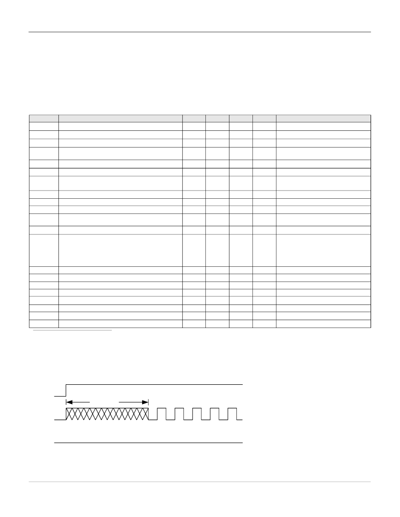
Figure 3-3. PLL Lock Timing Diagram
Table 3-18. AC Chip-Level Specifications
Symbol
F
IMO
F
CPU1
F
CPU2
F
48M
Description
Min
Typ
Max
Units
MHz
Notes
Internal Main Oscillator Frequency
23.4
24
24.6
a
24.6
a,b
12.3
b,c
49.2
a,b,d
Trimmed. Utilizing factory trim values.
CPU Frequency (5V Nominal)
0.93
24
a. 4.75V < Vdd < 5.25V.
b. Accuracy derived fromInternal Main Oscillator with appropriate trimfor Vdd range.
c. 3.0V < Vdd < 3.6V. See Application Note AN2012 “Adjusting PSoC Microcontroller Trims for Dual Voltage-Range Operation” for information on trimmng for operation at 3.3V.
d. See the individual user module data sheets for information on maximumfrequencies for user modules.
MHz
Trimmed. Utilizing factory trim values.
CPU Frequency (3.3V Nominal)
0.93
12
MHz
Trimmed. Utilizing factory trim values.
Digital PSoC Block Frequency
0
48
MHz
Refer to the AC Digital Block Specifications
below.
F
24M
F
32K1
F
32K2
Digital PSoC Block Frequency
0
24
24.6
b, d
64
MHz
Internal Low Speed Oscillator Frequency
15
32
kHz
External Crystal Oscillator
–
32.768
–
kHz
Accuracy is capacitor and crystal dependent.
50% duty cycle.
Multiple (x732) of crystal frequency.
F
PLL
Jitter24M2
T
PLLSLEW
T
PLLSLEWS-
LOW
T
OS
T
OSACC
PLL Frequency
–
23.986
–
MHz
24 MHz Period Jitter (PLL)
PLL Lock Time
–
0.5
–
–
600
10
ps
ms
PLL Lock Time for Low Gain Setting
0.5
–
50
ms
External Crystal Oscillator Startup to 1%
–
1700
2620
3800
ms
External Crystal Oscillator Startup to 100 ppm
–
2800
ms
The crystal oscillator frequency is within 100 ppmof its
final value by the end of the T
osacc
period. Correct
operation assumes a properly loaded 1 uW maximum
drive level 32.768 kHz crystal. 3.0V
≤
Vdd
≤
5.5V, -40
o
C
≤
T
A
≤
85
o
C.
Jitter32k
T
XRST
DC24M
Step24M
Fout48M
32 kHz Period Jitter
External Reset Pulse Width
–
10
100
–
ns
μ
s
%
kHz
MHz
–
24 MHz Duty Cycle
24 MHz Trim Step Size
48 MHz Output Frequency
40
–
46.8
50
50
48.0
60
–
49.2
a,c
Trimmed. Utilizing factory trim values.
Jitter24M1
F
MAX
T
RAMP
24 MHz Period Jitter (IMO)
Maximum frequency of signal on row input or row output.
–
–
600
–
ps
MHz
12.3
Supply Ramp Time
0
–
–
μ
s
24 MHz
F
PLL
PLL
Enable
T
PLLSLEW
PLL
Gain
0
相關(guān)PDF資料 |
PDF描述 |
|---|---|
| CY8C27243-24PVXIT | PSoC Mixed Signal Array |
| CY8C27443-24PVXIT | PSoC Mixed Signal Array |
| CY8C27243-24PVXI | PSoC Mixed Signal Array |
| CY8C27443-24PVXI | PSoC Mixed Signal Array |
| CY8C27543-24AIT | PSoC Mixed Signal Array |
相關(guān)代理商/技術(shù)參數(shù) |
參數(shù)描述 |
|---|---|
| CY8C276434-24PVXI | 功能描述:PROGRAMMABLE SYSTEM ON A CHIP RoHS:是 類別:未定義的類別 >> 其它 系列:* 標準包裝:1 系列:* 其它名稱:MS305720A |
| CY8C276435-24PVXI | 制造商:Cypress Semiconductor 功能描述: |
| CY8C27666-24PVXI | 制造商:Cypress Semiconductor 功能描述: |
| CY8C28000-24PVXI | 制造商:Cypress Semiconductor 功能描述: |
| CY8C28243-24PVXI | 功能描述:可編程片上系統(tǒng) - PSoC PSoC Programmable System-on-Chip RoHS:否 制造商:Cypress Semiconductor 核心:8051 處理器系列:CY8C36 數(shù)據(jù)總線寬度:8 bit 最大時鐘頻率:67 MHz 程序存儲器大小:32 KB 數(shù)據(jù) RAM 大小:4 KB 片上 ADC:Yes 工作電源電壓:0.5 V to 5.5 V 工作溫度范圍:- 40 C to + 85 C 封裝 / 箱體:QFN-68 安裝風(fēng)格:SMD/SMT |
發(fā)布緊急采購,3分鐘左右您將得到回復(fù)。