- 您現(xiàn)在的位置:買賣IC網(wǎng) > PDF目錄379098 > CY8C27443-24PVIT (CYPRESS SEMICONDUCTOR CORP) PSoC Mixed Signal Array PDF資料下載
參數(shù)資料
| 型號: | CY8C27443-24PVIT |
| 廠商: | CYPRESS SEMICONDUCTOR CORP |
| 元件分類: | 外設(shè)及接口 |
| 英文描述: | PSoC Mixed Signal Array |
| 中文描述: | MULTIFUNCTION PERIPHERAL, PDSO28 |
| 封裝: | 0.210 INCH, LEAD FREE, SSOP-28 |
| 文件頁數(shù): | 23/44頁 |
| 文件大小: | 542K |
| 代理商: | CY8C27443-24PVIT |
第1頁第2頁第3頁第4頁第5頁第6頁第7頁第8頁第9頁第10頁第11頁第12頁第13頁第14頁第15頁第16頁第17頁第18頁第19頁第20頁第21頁第22頁當前第23頁第24頁第25頁第26頁第27頁第28頁第29頁第30頁第31頁第32頁第33頁第34頁第35頁第36頁第37頁第38頁第39頁第40頁第41頁第42頁第43頁第44頁
August 3, 2004
Document No. 38-12012 Rev. *I
23
CY8C27x43 Final Data Sheet
3. Electrical Specifications
3.3.5
DC Switch Mode Pump Specifications
The following table lists guaranteed maximum and minimum specifications for the voltage and temperature ranges: 4.75V to 5.25V
and -40
°
C
≤
T
A
≤
85
°
C, or 3.0V to 3.6V and -40
°
C
≤
T
A
≤
85
°
C, respectively. Typical parameters apply to 5V and 3.3V at 25
°
C and
are for design guidance only.
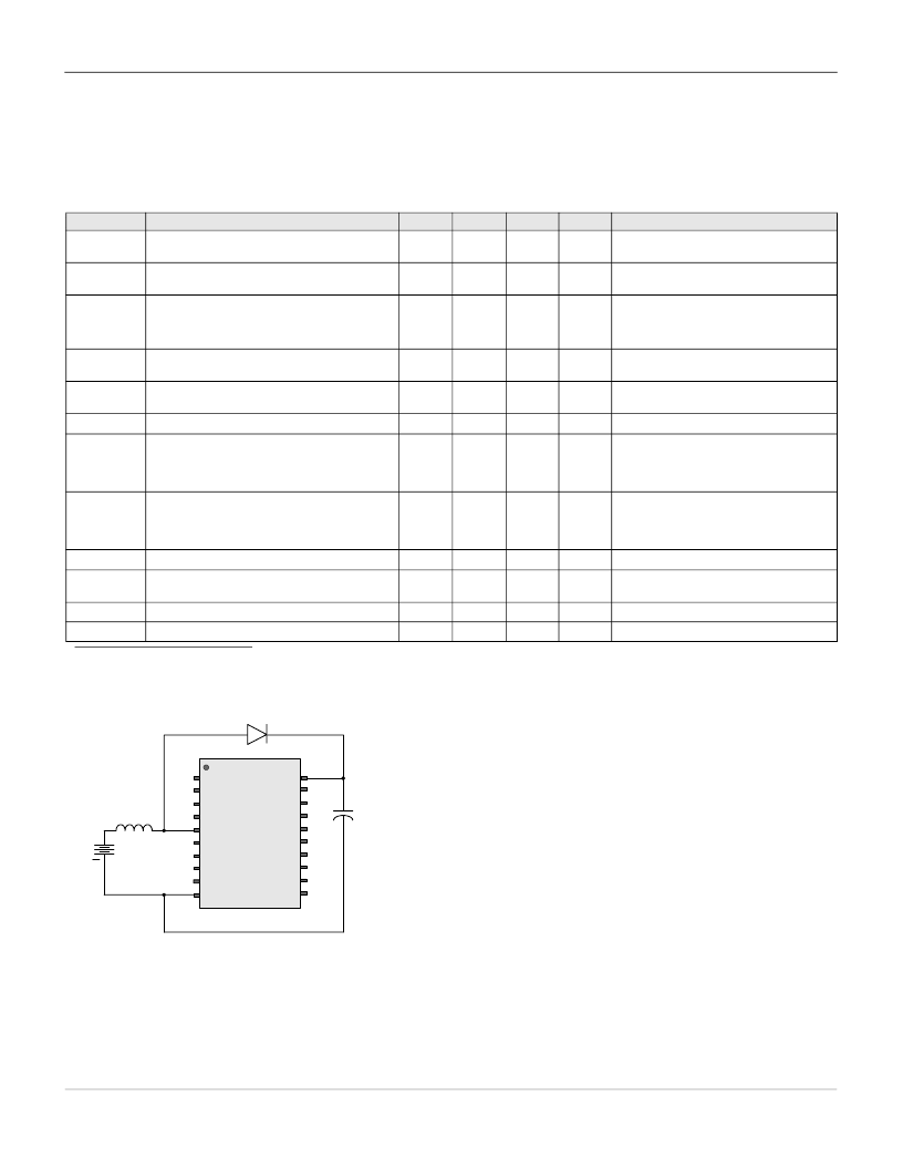
Figure 3-2. Basic Switch Mode Pump Circuit
Table 3-10. DC Switch Mode Pump (SMP) Specifications
Symbol
Description
Min
Typ
Max
Units
Notes
V
PUMP
5V
5V Output Voltage
4.75
5.0
5.25
V
Configuration of footnote
a
. Average, neglecting
ripple. SMP trip voltage is set to 5.0V.
a. L
1
= 2
μ
H inductor, C
1
= 10
μ
F capacitor, D
1
= Schottky diode. See Figure3-2.
V
PUMP
3V
3V Output Voltage
3.00
3.25
3.60
V
Configuration of footnote
a
. Average, neglecting
ripple. SMP trip voltage is set to 3.25V.
I
PUMP
Available Output Current
V
BAT
= 1.5V, V
PUMP
= 3.25V
V
BAT
= 1.8V, V
PUMP
= 5.0V
8
5
–
–
–
–
mA
mA
Configuration of footnote
a
.
SMP trip voltage is set to 3.25V.
SMP trip voltage is set to 5.0V.
V
BAT
5V
Input Voltage Range from Battery
1.8
–
5.0
V
Configuration of footnote
a
. SMP trip voltage is
set to 5.0V.
V
BAT
3V
Input Voltage Range from Battery
1.0
–
3.3
V
Configuration of footnote
a
. SMP trip voltage is
set to 3.25V.
V
BATSTART
Minimum Input Voltage from Battery to Start Pump
1.1
–
–
V
Configuration of footnote
a
.
V
PUMP_Line
Line Regulation (over V
BAT
range)
–
5
–
%V
O
Configuration of footnote
a
. V
O
is the “Vdd
Value for PUMP Trip” specified by the VM[2:0]
setting in the DC POR and LVD Specification,
Table 3-16 on page 26
.
V
PUMP_Load
Load Regulation
–
5
–
%V
O
Configuration of footnote
a
. V
O
is the “Vdd
Value for PUMP Trip” specified by the VM[2:0]
setting in the DC POR and LVD Specification,
Table 3-16 on page 26
.
V
PUMP_Ripple
Output Voltage Ripple (depends on capacitor/load)
–
100
–
mVpp
Configuration of footnote
a
. Load is 5mA.
E
3
Efficiency
35
50
–
%
Configuration of footnote
a
. Load is 5 mA. SMP
trip voltage is set to 3.25V.
F
PUMP
Switching Frequency
–
1.3
–
MHz
DC
PUMP
Switching Duty Cycle
–
50
–
%
Battery
C1
D1
+
PSoC
TM
Vdd
Vss
SMP
V
BAT
V
PUMP
L
1
相關(guān)PDF資料 |
PDF描述 |
|---|---|
| CY8C27443-24PXI | PSoC Mixed Signal Array |
| CY9C62256-70PC | 32K x 8 Magnetic Nonvolatile CMOS RAM |
| CY9C62256-70SC | 32K x 8 Magnetic Nonvolatile CMOS RAM |
| CY9C62256-70ZC | 32K x 8 Magnetic Nonvolatile CMOS RAM |
| CY9C62256-70ZI | 32K x 8 Magnetic Nonvolatile CMOS RAM |
相關(guān)代理商/技術(shù)參數(shù) |
參數(shù)描述 |
|---|---|
| CY8C27443-24PVXI | 功能描述:可編程片上系統(tǒng) - PSoC IC MCU 16K FLSH 256B SRAM RoHS:否 制造商:Cypress Semiconductor 核心:8051 處理器系列:CY8C36 數(shù)據(jù)總線寬度:8 bit 最大時鐘頻率:67 MHz 程序存儲器大小:32 KB 數(shù)據(jù) RAM 大小:4 KB 片上 ADC:Yes 工作電源電壓:0.5 V to 5.5 V 工作溫度范圍:- 40 C to + 85 C 封裝 / 箱體:QFN-68 安裝風(fēng)格:SMD/SMT |
| CY8C27443-24PVXIT | 功能描述:可編程片上系統(tǒng) - PSoC 16K FlSh 256B RAM IND RoHS:否 制造商:Cypress Semiconductor 核心:8051 處理器系列:CY8C36 數(shù)據(jù)總線寬度:8 bit 最大時鐘頻率:67 MHz 程序存儲器大小:32 KB 數(shù)據(jù) RAM 大小:4 KB 片上 ADC:Yes 工作電源電壓:0.5 V to 5.5 V 工作溫度范圍:- 40 C to + 85 C 封裝 / 箱體:QFN-68 安裝風(fēng)格:SMD/SMT |
| CY8C27443-24PXI | 功能描述:可編程片上系統(tǒng) - PSoC IC MCU 16K FLASH 256B SRAM RoHS:否 制造商:Cypress Semiconductor 核心:8051 處理器系列:CY8C36 數(shù)據(jù)總線寬度:8 bit 最大時鐘頻率:67 MHz 程序存儲器大小:32 KB 數(shù)據(jù) RAM 大小:4 KB 片上 ADC:Yes 工作電源電壓:0.5 V to 5.5 V 工作溫度范圍:- 40 C to + 85 C 封裝 / 箱體:QFN-68 安裝風(fēng)格:SMD/SMT |
| CY8C27443-24PXIES | 制造商:Cypress Semiconductor 功能描述: |
| CY8C27443-24SXI | 功能描述:可編程片上系統(tǒng) - PSoC IC MCU 16K FLSH 256B SRAM RoHS:否 制造商:Cypress Semiconductor 核心:8051 處理器系列:CY8C36 數(shù)據(jù)總線寬度:8 bit 最大時鐘頻率:67 MHz 程序存儲器大小:32 KB 數(shù)據(jù) RAM 大小:4 KB 片上 ADC:Yes 工作電源電壓:0.5 V to 5.5 V 工作溫度范圍:- 40 C to + 85 C 封裝 / 箱體:QFN-68 安裝風(fēng)格:SMD/SMT |
發(fā)布緊急采購,3分鐘左右您將得到回復(fù)。