- 您現(xiàn)在的位置:買賣IC網(wǎng) > PDF目錄379088 > CY7C1528V18 (Cypress Semiconductor Corp.) RAM9 QDR-I/DDR-I/QDR-II/DDR- II Errata PDF資料下載
參數(shù)資料
| 型號: | CY7C1528V18 |
| 廠商: | Cypress Semiconductor Corp. |
| 英文描述: | RAM9 QDR-I/DDR-I/QDR-II/DDR- II Errata |
| 中文描述: | RAM9 QDR-I/DDR-I/QDR-II/DDR-二勘誤表 |
| 文件頁數(shù): | 4/8頁 |
| 文件大?。?/td> | 217K |
| 代理商: | CY7C1528V18 |
Document #: 001-06217 Rev. *C
Page 4 of 8
ISSUE DEFINITION
This issue involves the output buffer entering an unidentified state when the input signals (only Control signals
or Clocks) are floating during reset or initialization of the memory controller after power up.
PARAMETERS AFFECTED
No timing parameters are affected. The device may drive the outputs even though the read operation is not
enabled. A dummy read is performed to clear this condition.
TRIGGER CONDITION(S)
Input signals(namely RPS# for QDR-I/QDRII , WE# and LD# for DDR-I/DDRII) or Clocks (K/K# and/or C/C#)
are floating during reset or initialization of the memory controller after power up.
SCOPE OF IMPACT
This issue will jeopardize any number of writes or reads
which take place after the controls or clock are left
floating. This can occur anywhere in the SRAM access ( all the way from power up of the memory device to
transitions taking place for read/write accesses to the memory device) if the above trigger conditions are met.
EXPLANATION OF ISSUE
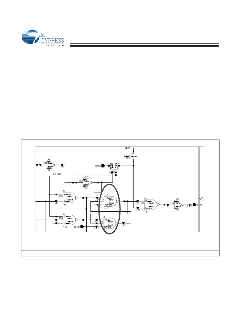
Figure 3
shows the output register Reset circuit with an SR Latch circled. This latch has two inputs with one
of them coming from some logic affected by the clock and RPS#(QDR) or WE# and LD#(DDR).The issue
happens when clocks are glitching/toggling with controls floating. This will cause the SR latch to be taken into
an unidentified state. The SR Latch will need to be reset by a dummy read operation if this happens.
WORKAROUND
This is viable only if the customer has the trigger conditions met during reset or initialization of the memory
controller after power up. In order for the workaround to perform properly, Cypress recommends the insertion
of a minimum of 16 “dummy” READ operations to every SRAM device on the board prior to writing any
meaningful data into the SRAM. After this one “dummy” READ operation, the device will perform properly.
“Dummy” READ is defined as a read operation to the device that is not meant to retrieve required data. The
“dummy” READ can be to any address location in the SRAM. Refer to
Figure 4
for the dummy read implemen-
tation.
Figure 3. Output Register Reset Circuit
SR LATCH
相關(guān)PDF資料 |
PDF描述 |
|---|---|
| CY7C1527V18-250BZXI | 72-Mbit DDR-II SRAM 2-Word Burst Architecture |
| CY7C1516V18-167BZC | 72-Mbit DDR-II SRAM 2-Word Burst Architecture |
| CY7C1516V18-167BZI | 72-Mbit DDR-II SRAM 2-Word Burst Architecture |
| CY7C1516V18-167BZXC | 72-Mbit DDR-II SRAM 2-Word Burst Architecture |
| CY7C1516V18-167BZXI | 72-Mbit DDR-II SRAM 2-Word Burst Architecture |
相關(guān)代理商/技術(shù)參數(shù) |
參數(shù)描述 |
|---|---|
| CY7C1543KV18-400BZC | 功能描述:靜態(tài)隨機存取存儲器 72MB (4Mx18) 1.8v 400MHz QDR II 靜態(tài)隨機存取存儲器 RoHS:否 制造商:Cypress Semiconductor 存儲容量:16 Mbit 組織:1 M x 16 訪問時間:55 ns 電源電壓-最大:3.6 V 電源電壓-最小:2.2 V 最大工作電流:22 uA 最大工作溫度:+ 85 C 最小工作溫度:- 40 C 安裝風格:SMD/SMT 封裝 / 箱體:TSOP-48 封裝:Tray |
| CY7C1543KV18-400BZI | 功能描述:靜態(tài)隨機存取存儲器 72MB (4Mx18) 1.8v 400MHz QDR II 靜態(tài)隨機存取存儲器 RoHS:否 制造商:Cypress Semiconductor 存儲容量:16 Mbit 組織:1 M x 16 訪問時間:55 ns 電源電壓-最大:3.6 V 電源電壓-最小:2.2 V 最大工作電流:22 uA 最大工作溫度:+ 85 C 最小工作溫度:- 40 C 安裝風格:SMD/SMT 封裝 / 箱體:TSOP-48 封裝:Tray |
| CY7C1543KV18-450BZC | 功能描述:靜態(tài)隨機存取存儲器 4Mb x 18 450 MHz RoHS:否 制造商:Cypress Semiconductor 存儲容量:16 Mbit 組織:1 M x 16 訪問時間:55 ns 電源電壓-最大:3.6 V 電源電壓-最小:2.2 V 最大工作電流:22 uA 最大工作溫度:+ 85 C 最小工作溫度:- 40 C 安裝風格:SMD/SMT 封裝 / 箱體:TSOP-48 封裝:Tray |
| CY7C1543KV18-450BZI | 功能描述:靜態(tài)隨機存取存儲器 72MB (8Mx9) 1.8v 450MHz QDR II 靜態(tài)隨機存取存儲器 RoHS:否 制造商:Cypress Semiconductor 存儲容量:16 Mbit 組織:1 M x 16 訪問時間:55 ns 電源電壓-最大:3.6 V 電源電壓-最小:2.2 V 最大工作電流:22 uA 最大工作溫度:+ 85 C 最小工作溫度:- 40 C 安裝風格:SMD/SMT 封裝 / 箱體:TSOP-48 封裝:Tray |
| CY7C1543V18-333BZC | 功能描述:靜態(tài)隨機存取存儲器 72M Q2+ B4 (2.0) RoHS:否 制造商:Cypress Semiconductor 存儲容量:16 Mbit 組織:1 M x 16 訪問時間:55 ns 電源電壓-最大:3.6 V 電源電壓-最小:2.2 V 最大工作電流:22 uA 最大工作溫度:+ 85 C 最小工作溫度:- 40 C 安裝風格:SMD/SMT 封裝 / 箱體:TSOP-48 封裝:Tray |
發(fā)布緊急采購,3分鐘左右您將得到回復(fù)。