- 您現(xiàn)在的位置:買賣IC網(wǎng) > PDF目錄379088 > CY7C1522V18 (Cypress Semiconductor Corp.) RAM9 QDR-I/DDR-I/QDR-II/DDR- II Errata PDF資料下載
參數(shù)資料
| 型號(hào): | CY7C1522V18 |
| 廠商: | Cypress Semiconductor Corp. |
| 英文描述: | RAM9 QDR-I/DDR-I/QDR-II/DDR- II Errata |
| 中文描述: | RAM9 QDR-I/DDR-I/QDR-II/DDR-二勘誤表 |
| 文件頁(yè)數(shù): | 2/8頁(yè) |
| 文件大小: | 217K |
| 代理商: | CY7C1522V18 |
Document #: 001-06217 Rev. *C
Page 2 of 8
Table 2. Issue Definition and fix status for different devices
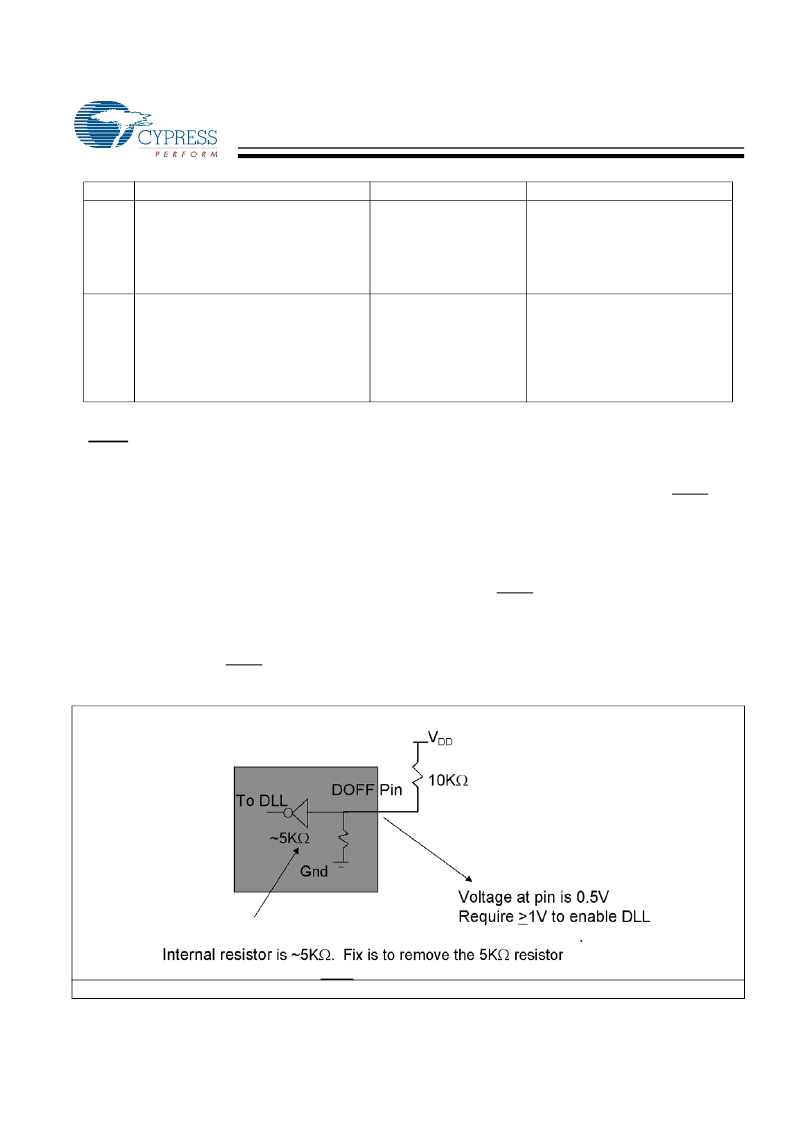
1. DOFF Pin Issue
ISSUE DEFINITION
This issue involves the DLL not turning ON properly if a large resistor is used (eg:-10K
resistor to enable the DLL. If a 10K
or higher pullup resistor is used externally, the voltage on DOFF is not
high enough to enable the DLL.
PARAMETERS AFFECTED
The functionality of the device will be affected because of the DLL is not turning ON properly. When the DLL
is enabled, all AC and DC parameters on the datasheet are met.
TRIGGER CONDITION(S)
Having a 10K
or higher external pullup resistor for disabling the DOFF pin.
SCOPE OF IMPACT
This issue will alter the normal functionality of the QDRII/DDRII devices when the DLL is disabled.
EXPLANATION OF ISSUE
Figure 1
shows the DOFF pin circuit with an internal 5K
internal 5K
leaker.
) as an external pullup
internal resistor. The fix planned is to disable the
WORKAROUND
2.
O/P Buffer enters a locked up unde-
fined state after controls or clocks are
left floating. No proper read/write
access can be done on the device
until a dummy read is performed.
9Mb - “D” Rev - Ram9
18Mb - “B” Rev - Ram9
36Mb - “A” Rev - Ram9
72Mb - Ram9
QDR-I/DDR-I/
QDR-II/DDR-II Devices
9Mb - “D” Rev - Ram9
18Mb - “B” Rev - Ram9
36Mb - “A” Rev - Ram9
72Mb - Ram9
The fix has been implemented on
the new revision and is now avail-
able.
3.
The EXTEST function in the JTAG
test fails when input K clock is floating
in the JTAG mode.
QDR-I/DDR-I/
QDR-II/DDR-II Devices
The fix involved bypassing the ZQ
circuitry in JTAG mode. This was
done by overriding the ZQ circuit-
ry by the JTAG signal. The fix has
been implemented on the new re-
vision and is now available.
Figure 1. DOFF pin with the 5K
internal resistor
Item
Issue
Device
Fix Status
相關(guān)PDF資料 |
PDF描述 |
|---|---|
| CY7C1524V18 | RAM9 QDR-I/DDR-I/QDR-II/DDR- II Errata |
| CY7C1528V18 | RAM9 QDR-I/DDR-I/QDR-II/DDR- II Errata |
| CY7C1527V18-250BZXI | 72-Mbit DDR-II SRAM 2-Word Burst Architecture |
| CY7C1516V18-167BZC | 72-Mbit DDR-II SRAM 2-Word Burst Architecture |
| CY7C1516V18-167BZI | 72-Mbit DDR-II SRAM 2-Word Burst Architecture |
相關(guān)代理商/技術(shù)參數(shù) |
參數(shù)描述 |
|---|---|
| CY7C1523AV18-200BZC | 功能描述:靜態(tài)隨機(jī)存取存儲(chǔ)器 4M x 18 1.8V DDR II SIO 靜態(tài)隨機(jī)存取存儲(chǔ)器 RoHS:否 制造商:Cypress Semiconductor 存儲(chǔ)容量:16 Mbit 組織:1 M x 16 訪問(wèn)時(shí)間:55 ns 電源電壓-最大:3.6 V 電源電壓-最小:2.2 V 最大工作電流:22 uA 最大工作溫度:+ 85 C 最小工作溫度:- 40 C 安裝風(fēng)格:SMD/SMT 封裝 / 箱體:TSOP-48 封裝:Tray |
| CY7C1523AV18-250BZC | 功能描述:靜態(tài)隨機(jī)存取存儲(chǔ)器 4M x 18 1.8V DDR II SIO 靜態(tài)隨機(jī)存取存儲(chǔ)器 RoHS:否 制造商:Cypress Semiconductor 存儲(chǔ)容量:16 Mbit 組織:1 M x 16 訪問(wèn)時(shí)間:55 ns 電源電壓-最大:3.6 V 電源電壓-最小:2.2 V 最大工作電流:22 uA 最大工作溫度:+ 85 C 最小工作溫度:- 40 C 安裝風(fēng)格:SMD/SMT 封裝 / 箱體:TSOP-48 封裝:Tray |
| CY7C1523JV18-300BZXC | 功能描述:靜態(tài)隨機(jī)存取存儲(chǔ)器 4Mbx18 72Mb 1.7-1.9V 300 MHz 2 WORD BURST RoHS:否 制造商:Cypress Semiconductor 存儲(chǔ)容量:16 Mbit 組織:1 M x 16 訪問(wèn)時(shí)間:55 ns 電源電壓-最大:3.6 V 電源電壓-最小:2.2 V 最大工作電流:22 uA 最大工作溫度:+ 85 C 最小工作溫度:- 40 C 安裝風(fēng)格:SMD/SMT 封裝 / 箱體:TSOP-48 封裝:Tray |
| CY7C1523KV18-250BZ | 制造商:Cypress Semiconductor 功能描述: |
| CY7C1523KV18-250BZXC | 功能描述:靜態(tài)隨機(jī)存取存儲(chǔ)器 72MB (4Mx18) 1.8v 250MHz DDR II 靜態(tài)隨機(jī)存取存儲(chǔ)器 RoHS:否 制造商:Cypress Semiconductor 存儲(chǔ)容量:16 Mbit 組織:1 M x 16 訪問(wèn)時(shí)間:55 ns 電源電壓-最大:3.6 V 電源電壓-最小:2.2 V 最大工作電流:22 uA 最大工作溫度:+ 85 C 最小工作溫度:- 40 C 安裝風(fēng)格:SMD/SMT 封裝 / 箱體:TSOP-48 封裝:Tray |
發(fā)布緊急采購(gòu),3分鐘左右您將得到回復(fù)。