- 您現(xiàn)在的位置:買賣IC網(wǎng) > PDF目錄379077 > CY7C1473V33-100BZXC (CYPRESS SEMICONDUCTOR CORP) 72-Mbit (2M x 36/4M x 18/1M x 72) Flow-Through SRAM with NoBL Architecture PDF資料下載
參數(shù)資料
| 型號(hào): | CY7C1473V33-100BZXC |
| 廠商: | CYPRESS SEMICONDUCTOR CORP |
| 元件分類: | DRAM |
| 英文描述: | 72-Mbit (2M x 36/4M x 18/1M x 72) Flow-Through SRAM with NoBL Architecture |
| 中文描述: | 4M X 18 ZBT SRAM, 8.5 ns, PBGA165 |
| 封裝: | 15 X 17 MM, 1.40 MM HEIGHT, LEAD FREE, FBGA-165 |
| 文件頁數(shù): | 10/29頁 |
| 文件大小: | 375K |
| 代理商: | CY7C1473V33-100BZXC |
第1頁第2頁第3頁第4頁第5頁第6頁第7頁第8頁第9頁當(dāng)前第10頁第11頁第12頁第13頁第14頁第15頁第16頁第17頁第18頁第19頁第20頁第21頁第22頁第23頁第24頁第25頁第26頁第27頁第28頁第29頁
PRELIMINARY
CY7C1471V33
CY7C1473V33
CY7C1475V33
Document #: 38-05288 Rev. *E
Page 10 of 29
Burst Write Accesses
The CY7C1471V33, CY7C1473V33, and CY7C1475V33
have an on-chip burst counter that allows the user the ability
to supply a single address and conduct up to four Write opera-
tions without reasserting the address inputs. ADV/LD must be
driven LOW in order to load the initial address, as described
in the Single Write Access section above. When ADV/LD is
driven HIGH on the subsequent clock rise, the Chip Enables
(CE
1
, CE
2
, and CE
3
) and WE inputs are ignored and the burst
counter is incremented. The correct BW
X
inputs must be
driven in each cycle of the burst write, in order to write the
correct bytes of data.
Sleep Mode
The ZZ input pin is an asynchronous input. Asserting ZZ
places the SRAM in a power conservation “sleep” mode. Two
clock cycles are required to enter into or exit from this “sleep”
mode. While in this mode, data integrity is guaranteed.
Accesses pending when entering the “sleep” mode are not
considered valid nor is the completion of the operation
guaranteed. The device must be deselected prior to entering
the “sleep” mode. CE
1
, CE
2
, and CE
3
, must remain inactive
for the duration of t
ZZREC
after the ZZ input returns LOW.
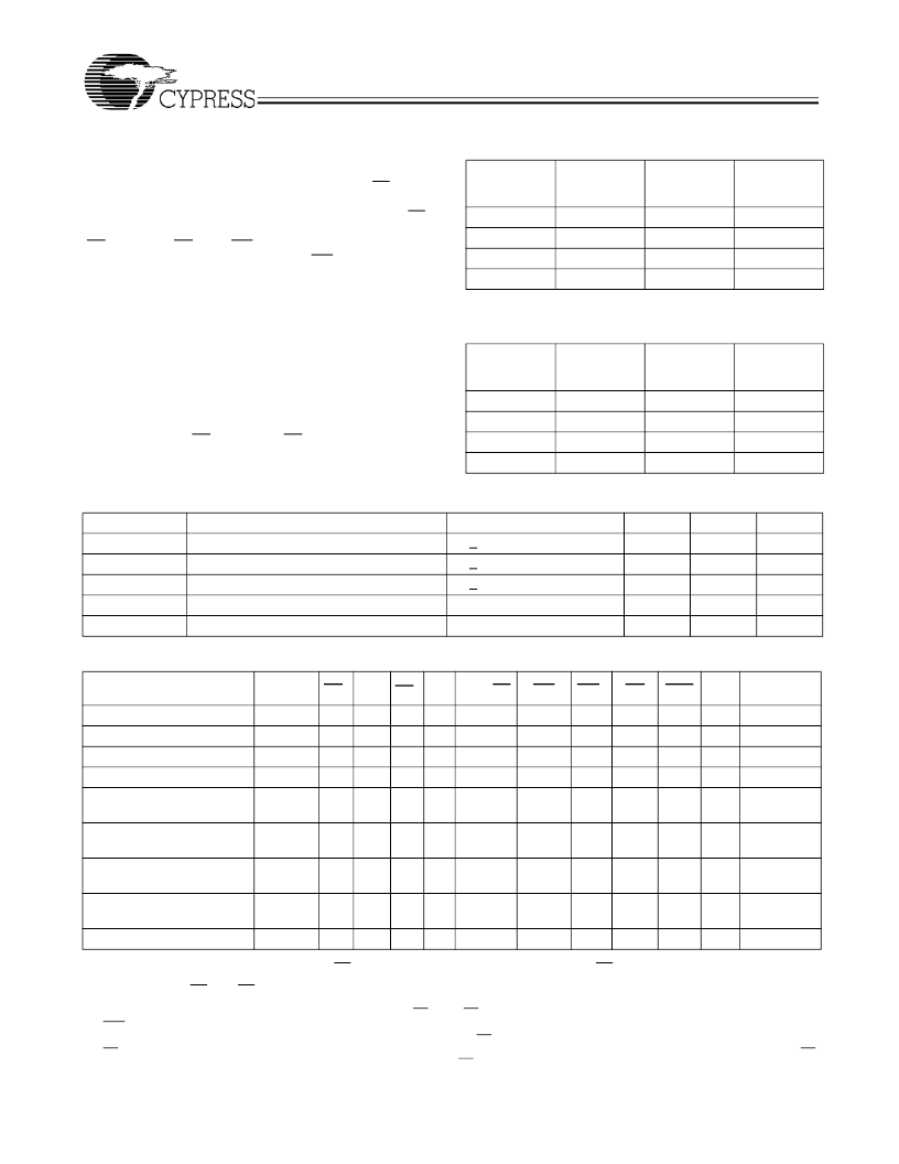
Truth Table
[2, 3, 4, 5, 6, 7, 8]
Interleaved Burst Address Table
(MODE = Floating or V
DD
)
First
Address
A1: A0
A1: A0
00
01
10
11
Second
Address
Third
Address
A1: A0
10
11
00
01
Fourth
Address
A1: A0
11
10
01
00
01
00
11
10
Linear Burst Address Table
(MODE = GND)
First
Address
A1: A0
00
01
10
11
Second
Address
A1: A0
01
10
11
00
Third
Address
A1: A0
10
11
00
01
Fourth
Address
A1: A0
11
00
01
10
ZZ Mode Electrical Characteristics
Parameter
I
DDZZ
t
ZZS
t
ZZREC
t
ZZI
t
RZZI
Description
Test Conditions
ZZ > V
DD
– 0.2V
ZZ > V
DD
– 0.2V
ZZ < 0.2V
This parameter is sampled
This parameter is sampled
Min.
Max.
150
2t
CYC
Unit
mA
ns
ns
ns
ns
Sleep mode standby current
Device operation to ZZ
ZZ recovery time
ZZ active to sleep current
ZZ Inactive to exit sleep current
2t
CYC
2t
CYC
0
Operation
Address
Used
None
None
None
None
External
CE
1
H
X
X
X
L
CE
2
CE
3
X
X
L
X
H
ZZ
L
L
L
L
L
ADV/LD
L
L
L
H
L
WE
X
X
X
X
H
BW
X
X
X
X
X
X
OE
X
X
X
X
L
CEN
L
L
L
L
L
CLK
L->H
L->H
L->H
L->H
L->H Data Out (Q)
DQ
Deselect Cycle
Deselect Cycle
Deselect Cycle
Continue Deselect Cycle
Read Cycle
(Begin Burst)
Read Cycle
(Continue Burst)
NOP/Dummy Read
(Begin Burst)
Dummy Read
(Continue Burst)
Write Cycle (Begin Burst)
X
H
X
X
L
Tri-State
Tri-State
Tri-State
Tri-State
Next
X
X
X
L
H
X
X
L
L
L->H Data Out (Q)
External
L
H
L
L
L
H
X
H
L
L->H
Tri-State
Next
X
X
X
L
H
X
X
H
L
L->H
Tri-State
External
L
H
L
L
L
L
L
X
L
L->H
Data In (D)
Notes:
2. X = “Don't Care.” H = Logic HIGH, L = Logic LOW. BWx = L signifies at least one Byte Write Select is active, BWx = Valid signifies that the desired Byte Write
Selects are asserted, see Truth Table for details.
3. Write is defined by BW
, and WE. See Truth Table for Read/Write.
4. When a Write cycle is detected, all I/Os are tri-stated, even during Byte Writes.
5. The DQs and DQP
X
pins are controlled by the current cycle and the OE signal. OE is asynchronous and is not sampled with the clock.
6. CEN = H, inserts wait states.
7. Device will power-up deselected and the I/Os in a tri-state condition, regardless of OE.
8. OE is asynchronous and is not sampled with the clock rise. It is masked internally during Write cycles. During a read cycle DQs and DQP
X
= Tri-state when OE
is inactive or when the device is deselected, and DQs and DQP
X
= data when OE is active.
相關(guān)PDF資料 |
PDF描述 |
|---|---|
| CY7C1473V33-133AXC | 72-Mbit (2M x 36/4M x 18/1M x 72) Flow-Through SRAM with NoBL Architecture |
| CY7C1473V33-133BZC | 72-Mbit (2M x 36/4M x 18/1M x 72) Flow-Through SRAM with NoBL Architecture |
| CY7C1471V33-100BZC | 72-Mbit (2M x 36/4M x 18/1M x 72) Flow-Through SRAM with NoBL Architecture |
| CY7C1471V33-100BZXC | LME Series; Mounting Style: Direct mount; Functions: Continuous light; Light Type: LED; Rated Voltage: 24V AC/DC; Style: 2 - light; Color: Red, Green (other color combo avail); Diameter: 60; Applicable Model: LME |
| CY7C1471V33-133BZXC | 72-Mbit (2M x 36/4M x 18/1M x 72) Flow-Through SRAM with NoBL Architecture |
相關(guān)代理商/技術(shù)參數(shù) |
參數(shù)描述 |
|---|---|
| CY7C1474BV25-167BGC | 功能描述:靜態(tài)隨機(jī)存取存儲(chǔ)器 1Mx72, 2.5V NoBL PL RoHS:否 制造商:Cypress Semiconductor 存儲(chǔ)容量:16 Mbit 組織:1 M x 16 訪問時(shí)間:55 ns 電源電壓-最大:3.6 V 電源電壓-最小:2.2 V 最大工作電流:22 uA 最大工作溫度:+ 85 C 最小工作溫度:- 40 C 安裝風(fēng)格:SMD/SMT 封裝 / 箱體:TSOP-48 封裝:Tray |
| CY7C1474BV25-167BGCT | 功能描述:靜態(tài)隨機(jī)存取存儲(chǔ)器 1Mx72, 2.5V NoBL PL RoHS:否 制造商:Cypress Semiconductor 存儲(chǔ)容量:16 Mbit 組織:1 M x 16 訪問時(shí)間:55 ns 電源電壓-最大:3.6 V 電源電壓-最小:2.2 V 最大工作電流:22 uA 最大工作溫度:+ 85 C 最小工作溫度:- 40 C 安裝風(fēng)格:SMD/SMT 封裝 / 箱體:TSOP-48 封裝:Tray |
| CY7C1474BV25-167BGI | 功能描述:靜態(tài)隨機(jī)存取存儲(chǔ)器 1Mx72, 2.5V NoBL PL RoHS:否 制造商:Cypress Semiconductor 存儲(chǔ)容量:16 Mbit 組織:1 M x 16 訪問時(shí)間:55 ns 電源電壓-最大:3.6 V 電源電壓-最小:2.2 V 最大工作電流:22 uA 最大工作溫度:+ 85 C 最小工作溫度:- 40 C 安裝風(fēng)格:SMD/SMT 封裝 / 箱體:TSOP-48 封裝:Tray |
| CY7C1474BV25-167BGIT | 功能描述:靜態(tài)隨機(jī)存取存儲(chǔ)器 1Mx72 2.5V NoBL PL 靜態(tài)隨機(jī)存取存儲(chǔ)器 RoHS:否 制造商:Cypress Semiconductor 存儲(chǔ)容量:16 Mbit 組織:1 M x 16 訪問時(shí)間:55 ns 電源電壓-最大:3.6 V 電源電壓-最小:2.2 V 最大工作電流:22 uA 最大工作溫度:+ 85 C 最小工作溫度:- 40 C 安裝風(fēng)格:SMD/SMT 封裝 / 箱體:TSOP-48 封裝:Tray |
| CY7C1474BV25-200BGC | 功能描述:靜態(tài)隨機(jī)存取存儲(chǔ)器 1Mx72, 2.5V NoBL PL RoHS:否 制造商:Cypress Semiconductor 存儲(chǔ)容量:16 Mbit 組織:1 M x 16 訪問時(shí)間:55 ns 電源電壓-最大:3.6 V 電源電壓-最小:2.2 V 最大工作電流:22 uA 最大工作溫度:+ 85 C 最小工作溫度:- 40 C 安裝風(fēng)格:SMD/SMT 封裝 / 箱體:TSOP-48 封裝:Tray |
發(fā)布緊急采購,3分鐘左右您將得到回復(fù)。