- 您現(xiàn)在的位置:買賣IC網(wǎng) > PDF目錄379087 > CY7C1411AV18 (Cypress Semiconductor Corp.) RAM9 QDR-I/DDR-I/QDR-II/DDR- II Errata PDF資料下載
參數(shù)資料
| 型號: | CY7C1411AV18 |
| 廠商: | Cypress Semiconductor Corp. |
| 英文描述: | RAM9 QDR-I/DDR-I/QDR-II/DDR- II Errata |
| 中文描述: | RAM9 QDR-I/DDR-I/QDR-II/DDR-二勘誤表 |
| 文件頁數(shù): | 5/8頁 |
| 文件大小: | 217K |
| 代理商: | CY7C1411AV18 |
Document #: 001-06217 Rev. *C
Page 5 of 8
In systems where multiple SRAMs with multiple RPS# lines are used, a dummy read operation will have to be
performed on every SRAM on the board. Below is an example sequence of events that can be performed
before valid access can be performed on the SRAM.
1) Initialize the Memory Controller
2) Assert RPS# Low for each of the memory devices
Note:
For all devices with x9 bus configuration, the following sequence needs to be performed:
1) For the 72M / 36M / 18M x9 devices drive address pin A2 / A10 / A3 low respectively and perform dummy
read.
2) For the 72M / 36M / 18M x9 devices drive address pin A2 / A10 / A3 high respectively and perform dummy
read.
If the customer has the trigger conditions met during normal access to the memory then there is no workaround
at this point.
FIX STATUS
The fix has been implemented on the new revision and is now available. The new revision is an increment of
the existing revision. Please refer to Table 4 for the list of devices affected, current revision and the new
revision after the fix.
3. JTAG Mode Issue
ISSUE DEFINITION
If the input clock (K Clock) is left floating when the device is in JTAG mode, spurious high frequency noise on
this input can be interpreted by the device as valid clocks. This could cause the impedance matching circuitry
(ZQ) on the QDR/DDR devices to periodically load itself with incorrect values. These incorrect values in the
ZQ register could force the outputs into a High-Impedance state. The ZQ circuitry requires at least 1000 valid
K clock cycles to drive the outputs from high impedance to low impedance levels.
PARAMETERS AFFECTED
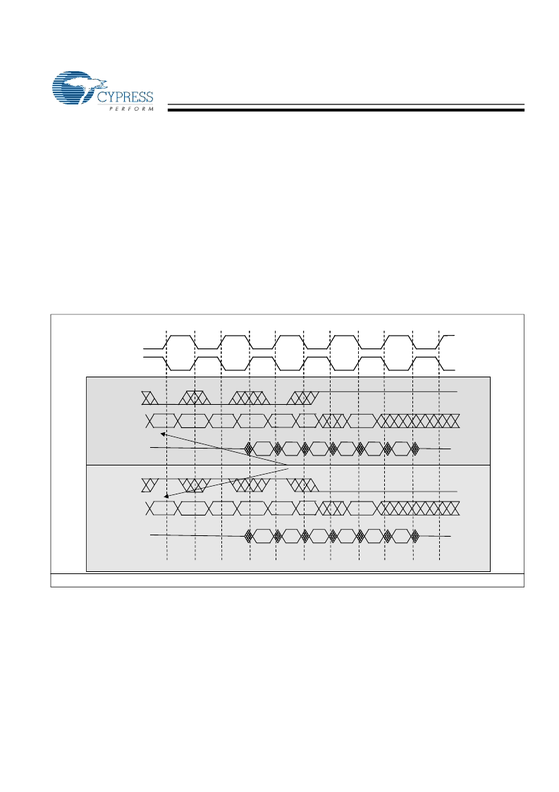
Figure 4. Dummy Read Implementation
/K
A
C
E
Q(A)
Q(A+1)
Q(C)
Q(C+1)
Q(E)
Q(E+1)
G
K
/RPS
Address
DataOut (Q)
A
C
E
DQ(A)
DQ
(A+1)
DQ(C)
DQ
(C+1)
DQ(E)
DQ
(E+1)
G
WE#
Address
DataOut (Q)
DDRII Operation
QDRII Operation
Dummy Read
相關(guān)PDF資料 |
PDF描述 |
|---|---|
| CY7C1413AV18 | RAM9 QDR-I/DDR-I/QDR-II/DDR- II Errata |
| CY7C1415AV18 | RAM9 QDR-I/DDR-I/QDR-II/DDR- II Errata |
| CY7C1416AV18 | RAM9 QDR-I/DDR-I/QDR-II/DDR- II Errata |
| CY7C1417AV18 | RAM9 QDR-I/DDR-I/QDR-II/DDR- II Errata |
| CY7C1418AV18 | RAM9 QDR-I/DDR-I/QDR-II/DDR- II Errata |
相關(guān)代理商/技術(shù)參數(shù) |
參數(shù)描述 |
|---|---|
| CY7C1411BV18-250BZC | 功能描述:靜態(tài)隨機存取存儲器 1Mx36 QDR II Burst 4 靜態(tài)隨機存取存儲器 RoHS:否 制造商:Cypress Semiconductor 存儲容量:16 Mbit 組織:1 M x 16 訪問時間:55 ns 電源電壓-最大:3.6 V 電源電壓-最小:2.2 V 最大工作電流:22 uA 最大工作溫度:+ 85 C 最小工作溫度:- 40 C 安裝風(fēng)格:SMD/SMT 封裝 / 箱體:TSOP-48 封裝:Tray |
| CY7C1411KV18-250BZC | 功能描述:靜態(tài)隨機存取存儲器 36Mb QDR II 靜態(tài)隨機存取存儲器 RoHS:否 制造商:Cypress Semiconductor 存儲容量:16 Mbit 組織:1 M x 16 訪問時間:55 ns 電源電壓-最大:3.6 V 電源電壓-最小:2.2 V 最大工作電流:22 uA 最大工作溫度:+ 85 C 最小工作溫度:- 40 C 安裝風(fēng)格:SMD/SMT 封裝 / 箱體:TSOP-48 封裝:Tray |
| CY7C1411KV18-300BZC | 功能描述:靜態(tài)隨機存取存儲器 36MB (4Mx8) 1.8v 300MHz QDR II 靜態(tài)隨機存取存儲器 RoHS:否 制造商:Cypress Semiconductor 存儲容量:16 Mbit 組織:1 M x 16 訪問時間:55 ns 電源電壓-最大:3.6 V 電源電壓-最小:2.2 V 最大工作電流:22 uA 最大工作溫度:+ 85 C 最小工作溫度:- 40 C 安裝風(fēng)格:SMD/SMT 封裝 / 箱體:TSOP-48 封裝:Tray |
| CY7C1411SC | 制造商:Cypress Semiconductor 功能描述: |
| CY7C1411SV18-250BZC | 功能描述:靜態(tài)隨機存取存儲器 NV靜態(tài)隨機存取存儲器 250 MHz 1.8V RoHS:否 制造商:Cypress Semiconductor 存儲容量:16 Mbit 組織:1 M x 16 訪問時間:55 ns 電源電壓-最大:3.6 V 電源電壓-最小:2.2 V 最大工作電流:22 uA 最大工作溫度:+ 85 C 最小工作溫度:- 40 C 安裝風(fēng)格:SMD/SMT 封裝 / 箱體:TSOP-48 封裝:Tray |
發(fā)布緊急采購,3分鐘左右您將得到回復(fù)。