- 您現(xiàn)在的位置:買賣IC網(wǎng) > PDF目錄379067 > CY7C1372D (Cypress Semiconductor Corp.) 18-Mbit (512K X 36/1M X 18) Pipelined SRAM with NoBL Architecture PDF資料下載
參數(shù)資料
| 型號: | CY7C1372D |
| 廠商: | Cypress Semiconductor Corp. |
| 英文描述: | 18-Mbit (512K X 36/1M X 18) Pipelined SRAM with NoBL Architecture |
| 中文描述: | 18兆位(為512k × 36/1M X 18)總線延遲架構(gòu)流水線的SRAM |
| 文件頁數(shù): | 8/30頁 |
| 文件大小: | 344K |
| 代理商: | CY7C1372D |
第1頁第2頁第3頁第4頁第5頁第6頁第7頁當(dāng)前第8頁第9頁第10頁第11頁第12頁第13頁第14頁第15頁第16頁第17頁第18頁第19頁第20頁第21頁第22頁第23頁第24頁第25頁第26頁第27頁第28頁第29頁第30頁
PRELIMINARY
CY7C1370D
CY7C1372D
Document #: 38-05555 Rev. *A
Page 8 of 30
outputs are active. The Output Enable (OE) can be deasserted
HIGH before presenting data to the DQ
and DQP
(DQ
a,b,c,d
/DQP
a,b,c,d
for CY7C1370D and DQ
a,b
/DQP
a,b
for
CY7C1372D) inputs. Doing so will three-state the output
drivers. As a safety precaution, DQ
and DQP (DQ
a,b,c,d
/
DQP
a,b,c,d
for
CY7C1370D
CY7C1372D) are automatically three-stated during the data
portion of a write cycle, regardless of the state of OE.
and
DQ
a,b
/DQP
a,b
for
Burst Write Accesses
The CY7C1370D/CY7C1372D has an on-chip burst counter
that allows the user the ability to supply a single address and
conduct up to four write operations without reasserting the
address inputs. ADV/LD must be driven LOW in order to load
the initial address, as described in the Single Write Access
section above. When ADV/LD is driven HIGH on the subse-
quent clock rise, the chip enables (CE
1
, CE
2
, and CE
3
) and
WE inputs are ignored and the burst counter is incremented.
The correct BW (BW
a,b,c,d
for CY7C1370D and BW
a,b
for
CY7C1372D) inputs must be driven in each cycle of the burst
write in order to write the correct bytes of data.
Sleep Mode
The ZZ input pin is an asynchronous input. Asserting ZZ
places the SRAM in a power conservation “sleep” mode. Two
clock cycles are required to enter into or exit from this “sleep”
mode. While in this mode, data integrity is guaranteed.
Accesses pending when entering the “sleep” mode are not
considered valid nor is the completion of the operation
guaranteed. The device must be deselected prior to entering
the “sleep” mode. CE
1
, CE
2
, and CE
3
, must remain inactive
for the duration of t
ZZREC
after the ZZ input returns LOW.
ZZ Mode Electrical Characteristics
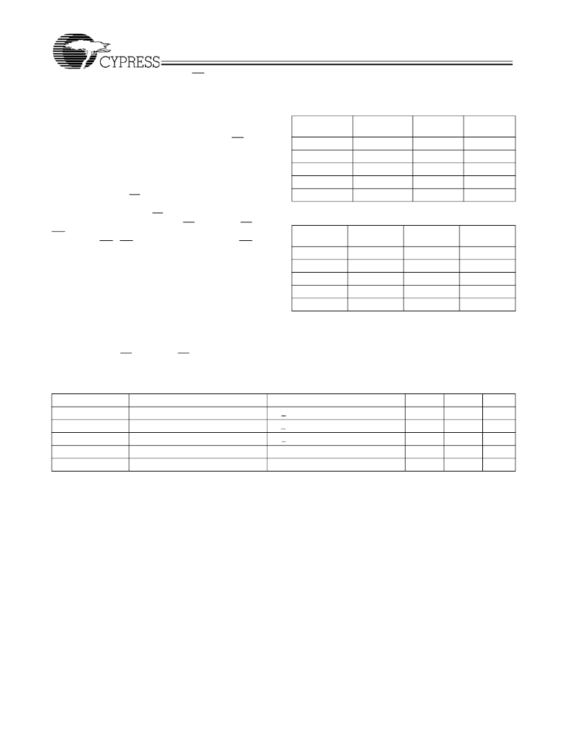
Linear Burst Address Table (MODE = GND)
Interleaved Burst Address Table
(MODE = Floating or V
DD
)
First
Address
Address
A1,A0
00
01
10
11
Second
Third
Address
A1,A0
10
11
00
01
Fourth
Address
A1,A0
11
10
01
00
A1,A0
01
00
11
10
First
Address
A1,A0
00
01
10
11
Second
Address
A1,A0
01
10
11
00
Third
Address
A1,A0
10
11
00
01
Fourth
Address
A1,A0
11
00
01
10
Parameter
I
DDZZ
t
ZZS
t
ZZREC
t
ZZI
t
RZZI
Description
Test Conditions
Min.
Max
80
2t
CYC
Unit
mA
ns
ns
ns
ns
Sleep mode standby current
Device operation to ZZ
ZZ recovery time
ZZ active to sleep current
ZZ Inactive to exit sleep current
ZZ
>
V
DD
0.2V
ZZ
>
V
DD
0.2V
ZZ
<
0.2V
This parameter is sampled
This parameter is sampled
2t
CYC
2t
CYC
0
相關(guān)PDF資料 |
PDF描述 |
|---|---|
| CY7C1372D-167AXC | 18-Mbit (512K X 36/1M X 18) Pipelined SRAM with NoBL Architecture |
| CY7C1372D-167AXI | 18-Mbit (512K X 36/1M X 18) Pipelined SRAM with NoBL Architecture |
| CY7C1372D-167BGC | 18-Mbit (512K X 36/1M X 18) Pipelined SRAM with NoBL Architecture |
| CY7C1372D-167BGI | 18-Mbit (512K X 36/1M X 18) Pipelined SRAM with NoBL Architecture |
| CY7C1372D-167BZC | 18-Mbit (512K X 36/1M X 18) Pipelined SRAM with NoBL Architecture |
相關(guān)代理商/技術(shù)參數(shù) |
參數(shù)描述 |
|---|---|
| CY7C1372D-167AXC | 功能描述:靜態(tài)隨機(jī)存取存儲器 1Mx18 3.3V NoBL Sync PL 靜態(tài)隨機(jī)存取存儲器 COM RoHS:否 制造商:Cypress Semiconductor 存儲容量:16 Mbit 組織:1 M x 16 訪問時間:55 ns 電源電壓-最大:3.6 V 電源電壓-最小:2.2 V 最大工作電流:22 uA 最大工作溫度:+ 85 C 最小工作溫度:- 40 C 安裝風(fēng)格:SMD/SMT 封裝 / 箱體:TSOP-48 封裝:Tray |
| CY7C1372D-167AXCT | 功能描述:靜態(tài)隨機(jī)存取存儲器 1Mx18 3.3V NoBL Sync PL 靜態(tài)隨機(jī)存取存儲器 COM RoHS:否 制造商:Cypress Semiconductor 存儲容量:16 Mbit 組織:1 M x 16 訪問時間:55 ns 電源電壓-最大:3.6 V 電源電壓-最小:2.2 V 最大工作電流:22 uA 最大工作溫度:+ 85 C 最小工作溫度:- 40 C 安裝風(fēng)格:SMD/SMT 封裝 / 箱體:TSOP-48 封裝:Tray |
| CY7C1372D-167AXI | 功能描述:靜態(tài)隨機(jī)存取存儲器 1Mx18 3.3V NoBL Sync PL 靜態(tài)隨機(jī)存取存儲器 IND RoHS:否 制造商:Cypress Semiconductor 存儲容量:16 Mbit 組織:1 M x 16 訪問時間:55 ns 電源電壓-最大:3.6 V 電源電壓-最小:2.2 V 最大工作電流:22 uA 最大工作溫度:+ 85 C 最小工作溫度:- 40 C 安裝風(fēng)格:SMD/SMT 封裝 / 箱體:TSOP-48 封裝:Tray |
| CY7C1372D-167AXIKJ | 制造商:Cypress Semiconductor 功能描述: |
| CY7C1372D-167AXIT | 功能描述:靜態(tài)隨機(jī)存取存儲器 1Mx18 3.3V NoBL Sync PL 靜態(tài)隨機(jī)存取存儲器 IND RoHS:否 制造商:Cypress Semiconductor 存儲容量:16 Mbit 組織:1 M x 16 訪問時間:55 ns 電源電壓-最大:3.6 V 電源電壓-最小:2.2 V 最大工作電流:22 uA 最大工作溫度:+ 85 C 最小工作溫度:- 40 C 安裝風(fēng)格:SMD/SMT 封裝 / 箱體:TSOP-48 封裝:Tray |
發(fā)布緊急采購,3分鐘左右您將得到回復(fù)。