- 您現(xiàn)在的位置:買(mǎi)賣(mài)IC網(wǎng) > PDF目錄379067 > CY7C1370C-250AC (CYPRESS SEMICONDUCTOR CORP) 512K x 36/1M x 18 Pipelined SRAM with NoBL Architecture PDF資料下載
參數(shù)資料
| 型號(hào): | CY7C1370C-250AC |
| 廠商: | CYPRESS SEMICONDUCTOR CORP |
| 元件分類: | DRAM |
| 英文描述: | 512K x 36/1M x 18 Pipelined SRAM with NoBL Architecture |
| 中文描述: | 512K X 36 ZBT SRAM, 2.6 ns, PQFP100 |
| 封裝: | 14 X 20 MM, 1.40 MM HEIGHT, PLASTIC, TQFP-100 |
| 文件頁(yè)數(shù): | 8/27頁(yè) |
| 文件大小: | 704K |
| 代理商: | CY7C1370C-250AC |
第1頁(yè)第2頁(yè)第3頁(yè)第4頁(yè)第5頁(yè)第6頁(yè)第7頁(yè)當(dāng)前第8頁(yè)第9頁(yè)第10頁(yè)第11頁(yè)第12頁(yè)第13頁(yè)第14頁(yè)第15頁(yè)第16頁(yè)第17頁(yè)第18頁(yè)第19頁(yè)第20頁(yè)第21頁(yè)第22頁(yè)第23頁(yè)第24頁(yè)第25頁(yè)第26頁(yè)第27頁(yè)
CY7C1370C
CY7C1372C
Document #: 38-05233 Rev. *D
Page 8 of 27
capability has been included in order to greatly simplify
Read/Modify/Write sequences, which can be reduced to
simple byte write operations.
Because the CY7C1370C and CY7C1372C are common I/O
devices, data should not be driven into the device while the
outputs are active. The Output Enable (OE) can be deasserted
HIGH before presenting data to the DQ
and DQP
(DQ
a,b,c,d
/DQP
a,b,c,d
for CY7C1370C and DQ
a,b
/DQP
a,b
for
CY7C1372C) inputs. Doing so will three-state the output
drivers. As a safety precaution, DQ
and DQP (DQ
a,b,c,d
/
DQP
a,b,c,d
for
CY7C1370C
CY7C1372C) are automatically three-stated during the data
portion of a write cycle, regardless of the state of OE.
and
DQ
a,b
/DQP
a,b
for
Burst Write Accesses
The CY7C1370C/CY7C1372C has an on-chip burst counter
that allows the user the ability to supply a single address and
conduct up to four WRITE operations without reasserting the
address inputs. ADV/LD must be driven LOW in order to load
the initial address, as described in the Single Write Access
section above. When ADV/LD is driven HIGH on the subse-
quent clock rise, the chip enables (CE
1
, CE
2
, and CE
3
) and
WE inputs are ignored and the burst counter is incremented.
The correct BW (BW
a,b,c,d
for CY7C1370C and BW
a,b
for
CY7C1372C) inputs must be driven in each cycle of the burst
write in order to write the correct bytes of data.
Sleep Mode
The ZZ input pin is an asynchronous input. Asserting ZZ
places the SRAM in a power conservation “sleep” mode. Two
clock cycles are required to enter into or exit from this “sleep”
mode. While in this mode, data integrity is guaranteed.
Accesses pending when entering the “sleep” mode are not
considered valid nor is the completion of the operation
guaranteed. The device must be deselected prior to entering
the “sleep” mode. CE
1
, CE
2
, and CE
3
, must remain inactive
for the duration of t
ZZREC
after the ZZ input returns LOW.
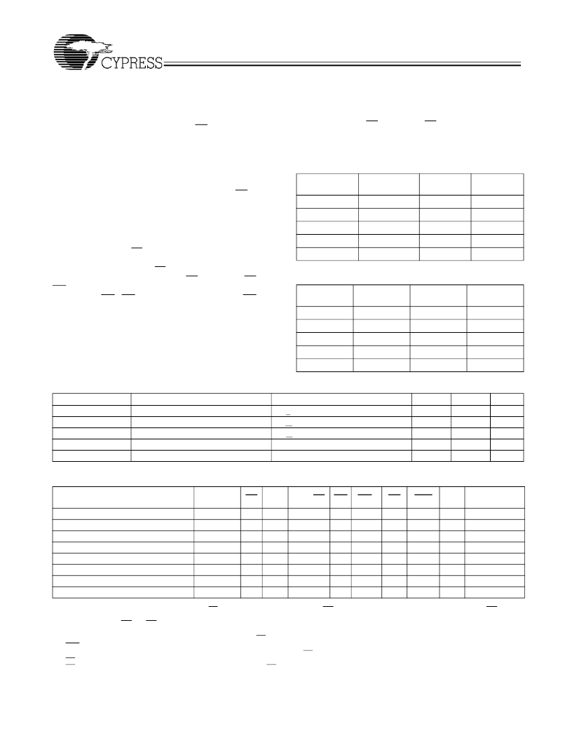
Interleaved Burst Address Table
(MODE = Floating or V
DD
)
First
Address
Address
A1,A0
A1,A0
00
01
01
00
10
11
11
10
Linear Burst Address Table (MODE = GND)
Second
Third
Address
A1,A0
10
11
00
01
Fourth
Address
A1,A0
11
10
01
00
First
Address
A1,A0
00
01
10
11
Second
Address
A1,A0
01
10
11
00
Third
Address
A1,A0
10
11
00
01
Fourth
Address
A1,A0
11
00
01
10
ZZ Mode Electrical Characteristics
Parameter
I
DDZZ
t
ZZS
t
ZZREC
t
ZZI
t
RZZI
Description
Test Conditions
Min.
Max
60
2t
CYC
Unit
mA
ns
ns
ns
ns
Snooze mode standby current
Device operation to ZZ
ZZ recovery time
ZZ active to snooze current
ZZ Inactive to exit snooze current
ZZ
>
V
DD
0.2V
ZZ
>
V
DD
0.2V
ZZ
<
0.2V
This parameter is sampled
This parameter is sampled
2t
CYC
2t
CYC
0
Truth Table
[1, 2, 3, 4, 5, 6, 7]
Operation
Address
Used
None
None
External
Next
External
Next
External
Next
CE
H
X
L
X
L
X
L
X
ZZ
L
L
L
L
L
L
L
L
ADV/LD
L
H
L
H
L
H
L
H
WE
X
X
H
X
H
X
L
X
BW
x
X
X
X
X
X
X
L
L
OE
X
X
L
L
H
H
X
X
CEN
L
L
L
L
L
L
L
L
CLK
L-H
L-H
L-H
L-H
L-H
L-H
L-H
L-H
DQ
Deselect Cycle
Continue Deselect Cycle
Read Cycle (Begin Burst)
Read Cycle (Continue Burst)
NOP/Dummy Read (Begin Burst)
Dummy Read (Continue Burst)
Write Cycle (Begin Burst)
Write Cycle (Continue Burst)
Notes:
1. X = “Don't Care”, 1 = Logic HIGH, 0 = Logic LOW, CE stands for ALL Chip Enables active. BWx = 0 signifies at least one Byte Write Select is active, BWx = Valid
signifies that the desired byte write selects are asserted, see Write Cycle Description table for details.
2. Write is defined by WE and BW
. See Write Cycle Description table for details.
3. When a write cycle is detected, all I/Os are tri-stated, even during byte writes.
4. The DQ and DQP pins are controlled by the current cycle and the OE signal.
5. CEN = H inserts wait states.
6. Device will power-up deselected and the I/Os in a tri-state condition, regardless of OE.
7. OE is asynchronous and is not sampled with the clock rise. It is masked internally during write cycles.During a read cycle DQ
s
and DQP
[a:d]
= Three-state when
OE is inactive or when the device is deselected, and DQ
s
=data when OE is active.
Three-State
Three-State
Data Out (Q)
Data Out (Q)
Three-State
Three-State
Data In (D)
Data In (D)
相關(guān)PDF資料 |
PDF描述 |
|---|---|
| CY7C1370C-250AI | 512K x 36/1M x 18 Pipelined SRAM with NoBL Architecture |
| CY7C1370C-250BGC | 512K x 36/1M x 18 Pipelined SRAM with NoBL Architecture |
| CY7C1370C-250BGI | 512K x 36/1M x 18 Pipelined SRAM with NoBL Architecture |
| CY7C1370C-250BZC | 512K x 36/1M x 18 Pipelined SRAM with NoBL Architecture |
| CY7C1370C-250BZI | 512K x 36/1M x 18 Pipelined SRAM with NoBL Architecture |
相關(guān)代理商/技術(shù)參數(shù) |
參數(shù)描述 |
|---|---|
| CY7C1370CV25-133AC | 制造商:Cypress Semiconductor 功能描述:16MB (512KX36) 2.5V NOBL-PIPE SRAM - Bulk |
| CY7C1370CV25-167AC | 制造商:Cypress Semiconductor 功能描述: |
| CY7C1370CV25167BZC | 制造商:Cypress Semiconductor 功能描述: |
| CY7C1370CV25-167BZI | 制造商:Cypress Semiconductor 功能描述: |
| CY7C1370D-167AXC | 功能描述:靜態(tài)隨機(jī)存取存儲(chǔ)器 512Kx36 3.3V NoBL Sync PL 靜態(tài)隨機(jī)存取存儲(chǔ)器 COM RoHS:否 制造商:Cypress Semiconductor 存儲(chǔ)容量:16 Mbit 組織:1 M x 16 訪問(wèn)時(shí)間:55 ns 電源電壓-最大:3.6 V 電源電壓-最小:2.2 V 最大工作電流:22 uA 最大工作溫度:+ 85 C 最小工作溫度:- 40 C 安裝風(fēng)格:SMD/SMT 封裝 / 箱體:TSOP-48 封裝:Tray |
發(fā)布緊急采購(gòu),3分鐘左右您將得到回復(fù)。