- 您現(xiàn)在的位置:買賣IC網(wǎng) > PDF目錄378496 > CY7C1041CV33-10ZSXA (CYPRESS SEMICONDUCTOR CORP) 4-Mbit (256K x 16) Static RAM PDF資料下載
參數(shù)資料
| 型號(hào): | CY7C1041CV33-10ZSXA |
| 廠商: | CYPRESS SEMICONDUCTOR CORP |
| 元件分類: | DRAM |
| 英文描述: | 4-Mbit (256K x 16) Static RAM |
| 中文描述: | 256K X 16 STANDARD SRAM, 10 ns, PDSO44 |
| 封裝: | LEAD FREE, TSOP2-44 |
| 文件頁(yè)數(shù): | 1/12頁(yè) |
| 文件大小: | 595K |
| 代理商: | CY7C1041CV33-10ZSXA |
4-Mbit (256K x 16) Static RAM
CY7C1041CV33
Cypress Semiconductor Corporation
Document #: 38-05134 Rev. *H
198 Champion Court
San Jose
,
CA 95134-1709
408-943-2600
Revised September 1, 2006
Features
Pin equivalent to CY7C1041BV33
Temperature Ranges
— Commercial: 0°C to 70°C
— Industrial: –40°C to 85°C
— Automotive-A: –40°C to 85°C
— Automotive-E: –40°C to 125°C
High speed
— t
AA
= 10 ns
Low active power
— 324 mW (max.)
2.0V data retention
Automatic power-down when deselected
TTL-compatible inputs and outputs
Easy memory expansion with CE and OE features
Available in Pb-free and non Pb-free 44-pin 400-mil-
SOJ, 44-pin TSOP II and 48-ball FBGA packages
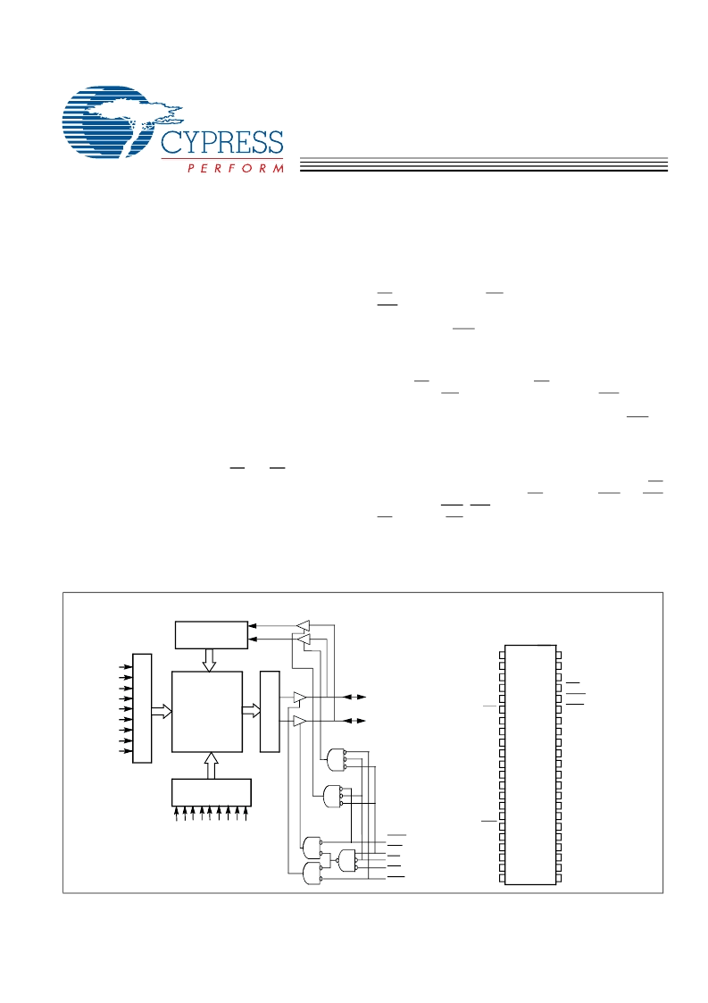
Functional Description
[1]
The CY7C1041CV33 is a high-performance CMOS Static
RAM organized as 262,144 words by 16 bits.
Writing to the device is accomplished by taking Chip Enable
(CE) and Write Enable (WE) inputs LOW. If Byte LOW Enable
(BLE) is LOW, then data from I/O pins (I/O
0
–I/O
7
), is written
into the location specified on the address pins (A
0
–A
17
). If Byte
HIGH Enable (BHE) is LOW, then data from I/O pins
(I/O
8
–I/O
15
) is written into the location specified on the
address pins (A
0
–A
17
).
Reading from the device is accomplished by taking Chip
Enable (CE) and Output Enable (OE) LOW while forcing the
Write Enable (WE) HIGH. If Byte LOW Enable (BLE) is LOW,
then data from the memory location specified by the address
pins will appear on I/O
0
– I/O
7
. If Byte HIGH Enable (BHE) is
LOW, then data from memory will appear on I/O
8
to I/O
15
. See
the truth table at the back of this data sheet for a complete
description of Read and Write modes.
The input/output pins (I/O
0
–I/O
15
) are placed in a
high-impedance state when the device is deselected (CE
HIGH), the outputs are disabled (OE HIGH), the BHE and BLE
are disabled (BHE, BLE HIGH), or during a Write operation
(CE LOW, and WE LOW).
The CY7C1041CV33 is available in a standard 44-pin
400-mil-wide body width SOJ and 44-pin TSOP II package
with center power and ground (revolutionary) pinout, as well
as a 48-ball fine-pitch ball grid array (FBGA) package.
Notes:
1. For guidelines on SRAM system design, please refer to the “System Design Guidelines” Cypress application note, available on the internet at www.cypress.com.
1
A
1
A
Logic Block Diagram
Pin Configuration
SOJ/
TSOP II
A
1
A
2
A
3
A
4
A
5
A
6
A
7
A
8
COLUMN
DECODER
R
S
INPUT BUFFER
256K × 16
ARRAY
A
0
A
1
A
1
A
1
A
1
A
1
A
9
A
1
I/O
0
–I/O
7
OE
BLE
I/O
8
–I/O
15
CE
WE
BHE
Top View
WE
A
5
A
6
A
7
A
8
A
9
1
2
3
4
5
6
7
8
9
10
11
12
13
14
15
31
30
32
36
35
34
33
37
40
39
38
41
44
43
42
16
17
29
28
V
CC
V
SS
I/O
4
I/O
5
A
0
A
1
A
2
A
3
A
4
OE
BHE
BLE
V
SS
V
CC
I/O
11
I/O
10
I/O
9
I/O
8
NC
A
17
A
16
A
15
I/O
15
I/O
14
I/O
13
I/O
12
CE
I/O
0
I/O
1
I/O
2
I/O
3
18
19
20
21
27
26
25
24
22
23
I/O
6
I/O
7
A
14
A
13
A
12
A
11
A
10
[+] Feedback
相關(guān)PDF資料 |
PDF描述 |
|---|---|
| CY7C1041CV33-10ZXC | 4-Mbit (256K x 16) Static RAM |
| CY7C1041CV33-10ZXI | 4-Mbit (256K x 16) Static RAM |
| CY7C1041CV33-12VXC | 4-Mbit (256K x 16) Static RAM |
| CY7C1041CV33-12VXI | 4-Mbit (256K x 16) Static RAM |
| CY7C1041CV33-12ZXC | 4-Mbit (256K x 16) Static RAM |
相關(guān)代理商/技術(shù)參數(shù) |
參數(shù)描述 |
|---|---|
| CY7C1041CV33-10ZSXAKJ | 制造商:Rochester Electronics LLC 功能描述: 制造商:Cypress Semiconductor 功能描述: |
| CY7C1041CV33-10ZSXAT | 功能描述:靜態(tài)隨機(jī)存取存儲(chǔ)器 256K x 16 3.3V R7 ASYNC 靜態(tài)隨機(jī)存取存儲(chǔ)器 RoHS:否 制造商:Cypress Semiconductor 存儲(chǔ)容量:16 Mbit 組織:1 M x 16 訪問(wèn)時(shí)間:55 ns 電源電壓-最大:3.6 V 電源電壓-最小:2.2 V 最大工作電流:22 uA 最大工作溫度:+ 85 C 最小工作溫度:- 40 C 安裝風(fēng)格:SMD/SMT 封裝 / 箱體:TSOP-48 封裝:Tray |
| CY7C1041CV33-10ZXC | 制造商:Cypress Semiconductor 功能描述:SRAM Chip Async Single 3.3V 4M-Bit 256K x 16 10ns 44-Pin TSOP-II |
| CY7C1041CV33-10ZXCT | 制造商:Cypress Semiconductor 功能描述:SRAM Chip Async Single 3.3V 4M-Bit 256K x 16 10ns 44-Pin TSOP-II T/R |
| CY7C1041CV33-10ZXI | 制造商:Cypress Semiconductor 功能描述:CYPCY7C1041CV33-10ZXI 4-MBIT (256K X 16) 制造商:Rochester Electronics LLC 功能描述: |
發(fā)布緊急采購(gòu),3分鐘左右您將得到回復(fù)。