- 您現(xiàn)在的位置:買賣IC網(wǎng) > PDF目錄378483 > CY62127DV30L (Cypress Semiconductor Corp.) 1 Mb (64K x 16) Static RAM PDF資料下載
參數(shù)資料
| 型號: | CY62127DV30L |
| 廠商: | Cypress Semiconductor Corp. |
| 英文描述: | 1 Mb (64K x 16) Static RAM |
| 中文描述: | 1字節(jié)(64K的× 16)靜態(tài)RAM |
| 文件頁數(shù): | 1/12頁 |
| 文件大小: | 384K |
| 代理商: | CY62127DV30L |
1 Mb (64K x 16) Static RAM
CY62127DV30
MoBL
Cypress Semiconductor Corporation
Document #: 38-05229 Rev. *D
3901 North First Street
San Jose
,
CA 95134
408-943-2600
Revised February 2, 2005
Features
Very high speed: 45 ns
Wide voltage range: 2.2V to 3.6V
Pin compatible with CY62127BV
Ultra-low active power
— Typical active current: 0.85 mA @ f = 1 MHz
— Typical active current: 5 mA @ f = f
MAX
Ultra-low standby power
Easy memory expansion with CE and OE features
Automatic power-down when deselected
Packages offered in a 48-ball FBGA and a 44-lead TSOP
Type II
Also available in Lead-Free 48-ball FBGA, and 44-lead
TSOP Type II packages
Functional Description
[1]
The CY62127DV30 is a high-performance CMOS static RAM
organized as 64K words by 16 bits. This device features
advanced circuit design to provide ultra-low active current.
This is ideal for providing More Battery Life
(MoBL
) in
portable applications such as cellular telephones. The device
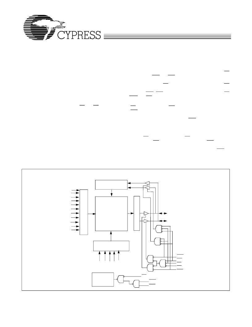
Logic Block Diagram
also has an automatic power-down feature that significantly
reduces power consumption by 90% when addresses are not
toggling. The device can be put into standby mode reducing
power consumption by more than 99% when deselected (CE
HIGH or both BHE and BLE are HIGH). The input/output pins
(I/O
0
through I/O
15
) are placed in a high-impedance state
when: deselected (CE HIGH), outputs are disabled (OE
HIGH), both Byte High Enable and Byte Low Enable are
disabled (BHE, BLE HIGH) or during a write operation (CE
LOW and WE LOW).
Writing to the device is accomplished by taking Chip Enable
(CE) and Write Enable (WE) inputs LOW. If Byte Low Enable
(BLE) is LOW, then data from I/O pins (I/O
0
through I/O
7
), is
written into the location specified on the address pins (A
0
through A
15
). If Byte High Enable (BHE) is LOW, then data
from I/O pins (I/O
8
through I/O
15
) is written into the location
specified on the address pins (A
0
through A
15
).
Reading from the device is accomplished by taking Chip
Enable (CE) and Output Enable (OE) LOW while forcing the
Write Enable (WE) HIGH. If Byte Low Enable (BLE) is LOW,
then data from the memory location specified by the address
pins will appear on I/O
0
to I/O
7
. If Byte High Enable (BHE) is
LOW, then data from memory will appear on I/O
8
to I/O
15
. See
the truth table at the back of this data sheet for a complete
description of read and write modes.
Note:
1. For best-practice recommendations, please refer to the Cypress application note “System Design Guidelines” on http://www.cypress.com.
64K x 16
RAM Array
2048 x 512
I/O
0
– I/O
7
R
A
8
A
7
A
6
A
5
A
4
A
3
A
2
A
1
COLUMN DECODER
A
1
A
1
A
1
A
1
A
1
S
DATA IN DRIVERS
OE
BLE
I/O
8
– I/O
15
CE
WE
BHE
A
0
A
9
Power
-
Down
Circuit
BHE
BLE
CE
A
10
相關(guān)PDF資料 |
PDF描述 |
|---|---|
| CY62127DV30L-55BVI | 1 Mb (64K x 16) Static RAM |
| CY62127BV | 64K x 16 Static RAM |
| CY62127BVLL-55BAI | 64K x 16 Static RAM |
| CY62127BVLL-55ZI | 64K x 16 Static RAM |
| CY62127BVLL-70BAI | 64K x 16 Static RAM |
相關(guān)代理商/技術(shù)參數(shù) |
參數(shù)描述 |
|---|---|
| CY62127DV30L-55BAI | 制造商:Cypress Semiconductor 功能描述:SRAM ASYNC SGL 2.5V/3.3V 1MBIT 64KX16 55NS 48FBGA - Bulk |
| CY62127DV30L-55BAIT | 制造商:Cypress Semiconductor 功能描述:SRAM ASYNC SGL 2.5V/3.3V 1MBIT 64KX16 55NS 48FBGA - Tape and Reel |
| CY62127DV30L-55BVI | 制造商:Cypress Semiconductor 功能描述: |
| CY62127DV30L-55BVXE | 功能描述:IC SRAM 1MBIT 55NS 48VFBGA RoHS:是 類別:集成電路 (IC) >> 存儲器 系列:MoBL® 標(biāo)準(zhǔn)包裝:1,000 系列:- 格式 - 存儲器:RAM 存儲器類型:移動 SDRAM 存儲容量:256M(8Mx32) 速度:133MHz 接口:并聯(lián) 電源電壓:1.7 V ~ 1.95 V 工作溫度:-40°C ~ 85°C 封裝/外殼:90-VFBGA 供應(yīng)商設(shè)備封裝:90-VFBGA(8x13) 包裝:帶卷 (TR) 其它名稱:557-1327-2 |
| CY62127DV30L-55BVXET | 功能描述:IC SRAM 1MBIT 55NS 48VFBGA RoHS:是 類別:集成電路 (IC) >> 存儲器 系列:MoBL® 標(biāo)準(zhǔn)包裝:1,000 系列:- 格式 - 存儲器:RAM 存儲器類型:移動 SDRAM 存儲容量:256M(8Mx32) 速度:133MHz 接口:并聯(lián) 電源電壓:1.7 V ~ 1.95 V 工作溫度:-40°C ~ 85°C 封裝/外殼:90-VFBGA 供應(yīng)商設(shè)備封裝:90-VFBGA(8x13) 包裝:帶卷 (TR) 其它名稱:557-1327-2 |
發(fā)布緊急采購,3分鐘左右您將得到回復(fù)。