- 您現(xiàn)在的位置:買賣IC網(wǎng) > PDF目錄384268 > CY26049-36 Clocks and Buffers PDF資料下載
參數(shù)資料
| 型號: | CY26049-36 |
| 英文描述: | Clocks and Buffers |
| 中文描述: | 時鐘和緩沖器 |
| 文件頁數(shù): | 2/6頁 |
| 文件大?。?/td> | 51K |
| 代理商: | CY26049-36 |
ADVANCE
INFORMATION
CY26049-1
Document #: 38-07488 Rev. *A
Page 2 of 6
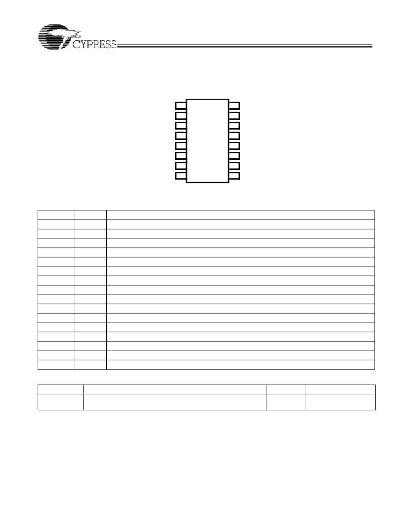
Pin Configuration
Description
CY26049-1 is a FailSafe frequency synthesizer with a
reference clock input and two 6.312-MHz outputs. The device
provides an optimum solution for applications where
continuous operation is required in the event of a primary clock
failure. The continuous, glitch-free operation is achieved by
using a DCXO, which serves as a primary clock source. The
FailSafe control circuit synchronizes the DCXO oscillator with
the reference as long as the reference is within the pull range
of the crystal.
In the event of a reference clock failure the DCXO maintains
the last frequency of the reference clock. The unique feature
of the CY26049-1 is that the DCXO is in fact the primary
clocking source. When the reference clock is restored, the
DCXO automatically resynchronizes to the reference. The
status of the reference clock input, as detected by the
CY26049-1, is reported by the SAFE pin.
Pin Description
Pin Number Pin Name
1
2
3
4
5
6
7
8
9
10
11
12
13
14
15
16
Pin Description
ICLK
NC
NC
NC
VDD
VSS
CLKA
XIN
XOUT
SAFE
VSS
VDD
NC
NC
CLKB
NC
Reference Input Clock
: 8kHz.
No Connect
.
No Connect
.
No Connect
.
Voltage Supply
: 3.3V.
Ground
.
Clock Output
: 6.312 MHz.
Pullable Crystal Input
: 18.432 MHz.
Pullable Crystal Output
: 18.432 MHz.
High = reference ICLK within range, Low = reference ICLK out of range
.
Ground
.
Voltage Supply
: 3.3V.
No Connect
.
No Connect
.
Clock Output
: 6.312 MHz.
No Connect
.
Selector Guide
Part Number
CY26049ZC-1 Reference Input Clock: 8 kHz
Crystal: 18.432-MHz pullable Crystal per Cypress Specification
Input Frequency Range
Outputs
2
Output Frequencies
6.312 MHz
CY26049-1
16-pin TSSOP
Top View
ICLK
1
16 NC
NC
2
15 CLKB
NC
3
14 NC
NC
4
13 NC
VDD
5
12 VDD
VSS
6
11 VSS
CLKA
7
10 SAFE
XIN
8
9 XOUT
相關(guān)PDF資料 |
PDF描述 |
|---|---|
| CY26049-5 | Clocks and Buffers |
| CY26111 | Clocks and Buffers |
| CY26111ZC | MISCELLANEOUS CLOCK GENERATOR|CMOS|TSSOP|16PIN|PLASTIC |
| CY26113 | Clocks and Buffers |
| CY26113ZC | MISCELLANEOUS CLOCK GENERATOR|CMOS|TSSOP|16PIN|PLASTIC |
相關(guān)代理商/技術(shù)參數(shù) |
參數(shù)描述 |
|---|---|
| CY26049-5 | 制造商:未知廠家 制造商全稱:未知廠家 功能描述:Clocks and Buffers |
| CY26049KZXI-36 | 制造商:Cypress Semiconductor 功能描述: |
| CY26049ZC-20 | 制造商:Rochester Electronics LLC 功能描述:- Bulk 制造商:Cypress Semiconductor 功能描述: |
| CY26049ZC-36 | 制造商:CYPRESS 制造商全稱:Cypress Semiconductor 功能描述:FailSafe⑩ PacketClock⑩ Global Communications Clock Generator |
| CY26049ZC-36T | 制造商:CYPRESS 制造商全稱:Cypress Semiconductor 功能描述:FailSafe⑩ PacketClock⑩ Global Communications Clock Generator |
發(fā)布緊急采購,3分鐘左右您將得到回復(fù)。