- 您現(xiàn)在的位置:買賣IC網(wǎng) > PDF目錄378999 > CY22800-048A (Cypress Semiconductor Corp.) Universal Programmable Clock Generator (UPCG) PDF資料下載
參數(shù)資料
| 型號(hào): | CY22800-048A |
| 廠商: | Cypress Semiconductor Corp. |
| 英文描述: | Universal Programmable Clock Generator (UPCG) |
| 中文描述: | 通用可編程時(shí)鐘發(fā)生器(UPCG) |
| 文件頁數(shù): | 1/10頁 |
| 文件大?。?/td> | 412K |
| 代理商: | CY22800-048A |
Universal Programmable Clock
Generator (UPCG)
CY22800
Cypress Semiconductor Corporation
Document #: 001-07704 Rev. *A
198 Champion Court
San Jose
,
CA 95134-1709
408-943-2600
Revised May 11, 2007
Features
Spread Spectrum, VCXO, and Frequency Select
Input frequency range:
— Crystal: 8–30 MHz
— CLKIN: 0.5–100 MHz
Output frequency:
— Commercial: 1–200 MHz
— Industrial: 1–166 MHz
Integrated phase-locked loop
Low jitter, high accuracy outputs
3.3V operation
8-pin SOIC package
Benefits
Inventory of only one device, CY22800, is needed in various
applications such as HDTV, STB, DVDR, etc.
Multiple predefined configurations that can be programmed
into a single chip
Eliminates the need for expensive and difficult to use
higher-order crystal
High-performance PLL tailored for multiple applications
Meets critical timing requirements in complex system
designs
Enables application compatibility
Allows up to three different frequency selects
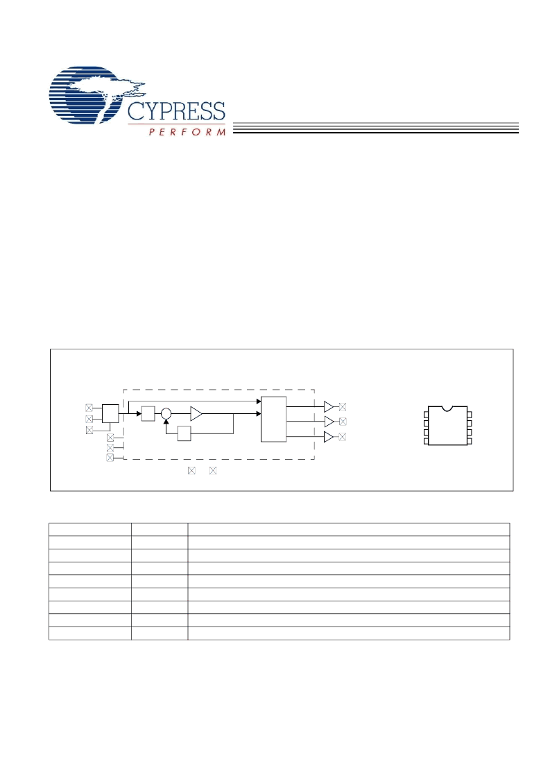
Logic Block Diagram
8-pin SOIC
1
2
3
4
XOUT
CLKB/FS1
VSS
CLKC/FS2/VSS
CLKA/FS0
5
6
7
8
VDD
XIN/CLKIN
FS0/VCXO
CY22800
Pin Configuration
XOUT
PLL
OSC
Q
P
VCO
VDD
VSS
Φ
CLKC
FS1
FS0
OUTPUT
DIVIDER
CLKB
(with modulation control)
XIN/CLKIN
CLKA
FS2
VCXO
Pin Description
Name
XIN
VDD
FS0/VCXO
VSS
CLKB/FS1
CLKA/FS0
CLKC/FS2/VSS
XOUT
Pin Number
1
2
3
4
5
6
7
8
Description
Reference Input; Crystal or External Clock
3.3V Voltage Supply
Frequency Select 0/VCXO Analog Control Voltage
[1]
Ground
Clock Output B/Frequency Select 1
[1]
Clock Output A/Frequency Select 0
[1]
Clock Output C/Frequency Select 2/VSS
[1]
Reference Output (No Connect when the reference is a clock)
Note
1. Pin definition changes for different configurations. Refer to the specific one-page data sheet for more details.
[+] Feedback
相關(guān)PDF資料 |
PDF描述 |
|---|---|
| CY22800-049A | Universal Programmable Clock Generator (UPCG) |
| CY22800-050A | Universal Programmable Clock Generator (UPCG) |
| CY22800-051A | Universal Programmable Clock Generator (UPCG) |
| CY22800-052A | Universal Programmable Clock Generator (UPCG) |
| CY22800-053A | Universal Programmable Clock Generator (UPCG) |
相關(guān)代理商/技術(shù)參數(shù) |
參數(shù)描述 |
|---|---|
| CY22800-049A | 制造商:CYPRESS 制造商全稱:Cypress Semiconductor 功能描述:Universal Programmable Clock Generator (UPCG) |
| CY22800-050A | 制造商:CYPRESS 制造商全稱:Cypress Semiconductor 功能描述:Universal Programmable Clock Generator (UPCG) |
| CY22800-051A | 制造商:CYPRESS 制造商全稱:Cypress Semiconductor 功能描述:Universal Programmable Clock Generator (UPCG) |
| CY22800-052A | 制造商:CYPRESS 制造商全稱:Cypress Semiconductor 功能描述:Universal Programmable Clock Generator (UPCG) |
| CY22800-053A | 制造商:CYPRESS 制造商全稱:Cypress Semiconductor 功能描述:Universal Programmable Clock Generator (UPCG) |
發(fā)布緊急采購,3分鐘左右您將得到回復(fù)。