- 您現在的位置:買賣IC網 > PDF目錄378996 > CXP88740 (Sony Corporation) CMOS 8-bit Single Chip Microcomputer PDF資料下載
參數資料
| 型號: | CXP88740 |
| 廠商: | Sony Corporation |
| 英文描述: | CMOS 8-bit Single Chip Microcomputer |
| 中文描述: | 的CMOS 8位單片機 |
| 文件頁數: | 1/32頁 |
| 文件大?。?/td> | 425K |
| 代理商: | CXP88740 |
當前第1頁第2頁第3頁第4頁第5頁第6頁第7頁第8頁第9頁第10頁第11頁第12頁第13頁第14頁第15頁第16頁第17頁第18頁第19頁第20頁第21頁第22頁第23頁第24頁第25頁第26頁第27頁第28頁第29頁第30頁第31頁第32頁
Description
The CXP88732/88740/88748 is a CMOS 8-bit
microcomputer which consists of A/D converter,
serial interface, timer/counter, time base timer, high
precision timing pattern generation circuits, PWM
output, VISS/ VASS circuit, 32kHz timer/counter,
remote control receiving circuit, VSYNC separator
and the measurement circuit which measure signals
of capstan FG amplifier and drum FG/PG amplifier
and other servo systems, as well as basic
configurations like 8-bit CPU, ROM, RAM and I/O
port. They are integrated into a single chip.
Also, CXP88732/88740/88748 provides sleep/stop
function which enables to lower power consumption.
Features
A wide instruction set (213 instructions) which cover various types of data
— 16-bit arithmetic/multiplication and division/boolean bit operation instructions
Minimum instruction cycle
250ns at 16MHz operation
122μs at 32kHz operation
Incorporated ROM capacity
32K bytes (CXP88732)
40K bytes (CXP88740)
48K bytes (CXP88748)
Incorporated RAM capacity
1344 bytes (including PPG RAM)
Peripheral function
— A/D converter
8 bits, 14 channels, successive approximation system
(Conversion time of 20μs/16MHz)
Incorporated 8-bit, 8-stage FIFO for data
(Auto transfer for 1 to 8 bytes), 1 channel
8-bit clock sync type, 1 channel
8-bit timer/counter, 2 channels
19-bit time base timer
32kHz timer/counter
PPG 19 pins 32-stage programmable circuit
RTG 5 pins, 1 channel
5-bit, 8-satge FIFO (RECCTL control), 1channel
12 bits, 2 channels (Repetitive frequency 62.5kHz/16MHz)
DA gate pulse output, 13 bits, 2 channels
Capstan FG amplifier circuit
Drum FG amplifier circuit
Drum PG amplifier circuit
PBCTL amplifier circuit
Recording current control circuit
Capstan FG, Drum FG/PG, CTL input
— Serial interface
— Timer
— High precision timing pattern generation
— PWM/DA gate output
— Analog signal input circuit
— CTL write/rewrite circuit
— Servo input control
— VSYNC separator
— FRC capture unit
— PWM output
— VISS/VASS circuit
— 32kHz timer/event counter
— Remote control reception circuit
— Tri-state output
— Pseudo HSYNC output function
— High speed head switching circuit
Interruption
Standby mode
Package
Piggyback/evaluation chip
Incorporated 26-bit and 8-stage FIFO
14-bit, 1 channel
Pulse duty auto detection circuit
32kHz oscillation circuit, ultra-low speed instruction mode
8-bit pulse measurement counter, 6-stage FIFO
PPG 1 pin, output 8 pins
20 factors, 15 vectors, multi-interruption possible
SLEEP/STOP
100-pin plastic QFP
CXP88800 100-pin ceramic QFP
– 1 –
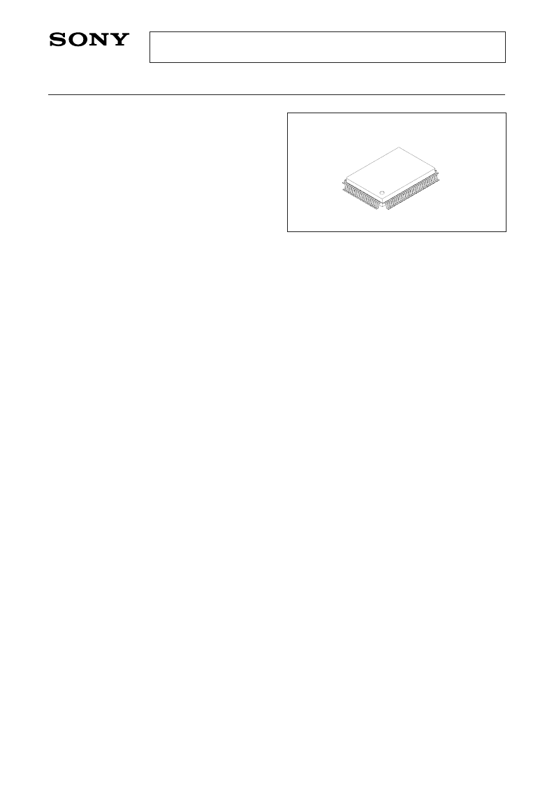
CXP88732/88740/88748
CMOS 8-bit Single Chip Microcomputer
100 pin QFP (Plastic)
E96109-ST
Sony reserves the right to change products and specifications without prior notice. This information does not convey any license by
any implication or otherwise under any patents or other right. Application circuits shown, if any, are typical examples illustrating the
operation of the devices. Sony cannot assume responsibility for any problems arising out of the use of these circuits.
Structure
Silicon gate CMOS IC
相關PDF資料 |
PDF描述 |
|---|---|
| CXP88748 | CMOS 8-bit Single Chip Microcomputer |
| CXP88732Q | 8-BIT MICROCONTROLLER |
| CXP88740Q | 8-BIT MICROCONTROLLER |
| CXP88748Q | 8-BIT MICROCONTROLLER |
| CXP88800 | CMOS 8-bit Single Chip Microcomputer |
相關代理商/技術參數 |
參數描述 |
|---|---|
| CXP88740Q | 制造商:SONY 制造商全稱:Sony Corporation 功能描述:8-Bit Microcontroller |
| CXP88748 | 制造商:SONY 制造商全稱:Sony Corporation 功能描述:CMOS 8-bit Single Chip Microcomputer |
| CXP88748Q | 制造商:SONY 制造商全稱:Sony Corporation 功能描述:8-Bit Microcontroller |
| CXP88800 | 制造商:SONY 制造商全稱:Sony Corporation 功能描述:CMOS 8-bit Single Chip Microcomputer |
| CXP88852 | 制造商:SONY 制造商全稱:Sony Corporation 功能描述:CMOS 8-bit Single Chip Microcomputer |
發(fā)布緊急采購,3分鐘左右您將得到回復。