- 您現(xiàn)在的位置:買賣IC網(wǎng) > PDF目錄378477 > CXP83621Q (Sony Corporation) Microcontroller PDF資料下載
參數(shù)資料
| 型號(hào): | CXP83621Q |
| 廠商: | Sony Corporation |
| 英文描述: | Microcontroller |
| 中文描述: | 微控制器 |
| 文件頁(yè)數(shù): | 23/30頁(yè) |
| 文件大?。?/td> | 423K |
| 代理商: | CXP83621Q |
第1頁(yè)第2頁(yè)第3頁(yè)第4頁(yè)第5頁(yè)第6頁(yè)第7頁(yè)第8頁(yè)第9頁(yè)第10頁(yè)第11頁(yè)第12頁(yè)第13頁(yè)第14頁(yè)第15頁(yè)第16頁(yè)第17頁(yè)第18頁(yè)第19頁(yè)第20頁(yè)第21頁(yè)第22頁(yè)當(dāng)前第23頁(yè)第24頁(yè)第25頁(yè)第26頁(yè)第27頁(yè)第28頁(yè)第29頁(yè)第30頁(yè)
– 23 –
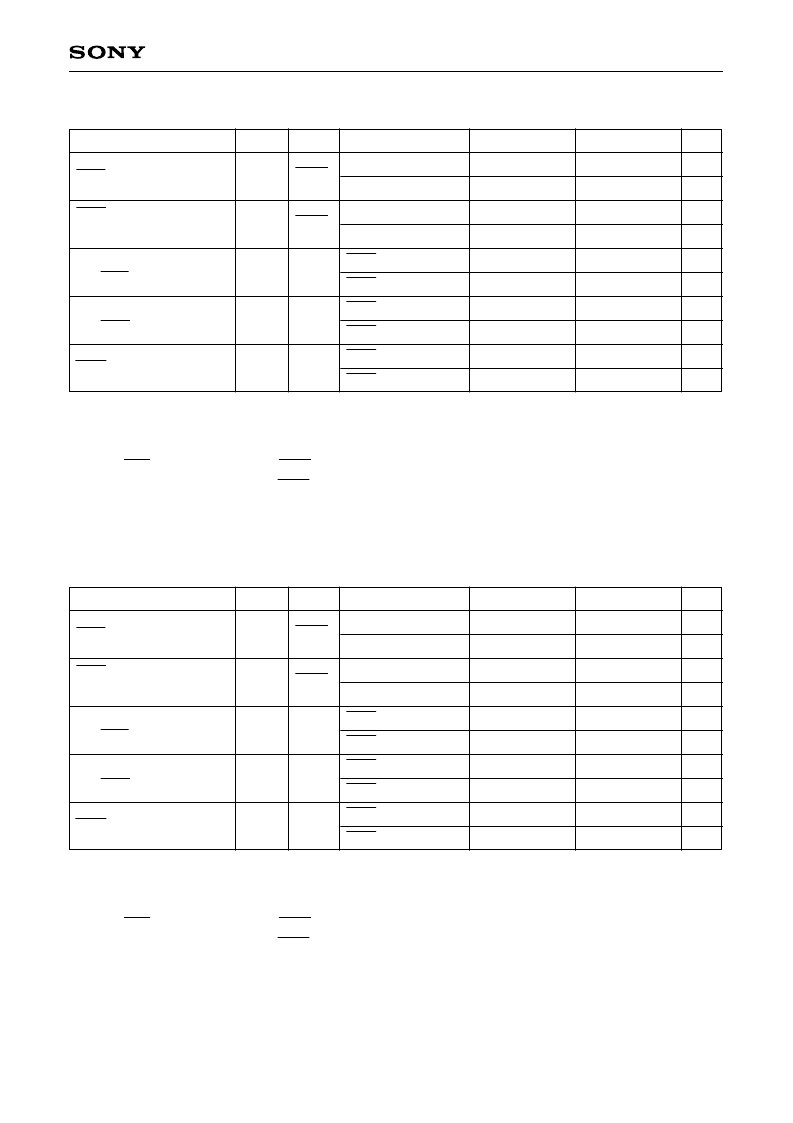
CXP83620/83624, CXP83621/83625
Serial Transfer (CH1)
(Ta = –20 to +75°C, V
DD
= 4.5 to 5.5V, Vss = 0V)
Item
SCK cycle time
t
KCY
SCK1
Input mode
Output mode
Input mode
Output mode
SCK input mode
SCK output mode
SCK input mode
SCK output mode
SCK input mode
SCK output mode
1000
8000/fc
400
4000/fc – 50
100
200
200
100
200
100
ns
ns
ns
ns
ns
ns
ns
ns
ns
ns
SCK1
SI1
SI1
SO1
t
KH
t
KL
t
SIK
t
KSI
t
KSO
SCK high and low level
widths
SI input setup time
(for SCK
↑
)
SI input hold time
(for SCK
↑
)
SCK
↓ →
SO delay time
Symbol
Pin
Conditions
Min.
Max.
Unit
Note 1)
t
sys indicates the three values below according to the upper two bits (CPU clock selection) of the
clock control register (CLC: 00FEh).
t
sys [ns] = 2000/fc (upper two bits = “00”), 4000/fc (upper two bits = “01”), 16000/fc (upper two bits = “11”)
Note 2)
SCK, SI and SO indicates SCK1, SI1 and SO1, respectively.
Note 3)
The load condition for the SCK1 output mode, SO1 output delay time is 50pF + 1TTL.
Note 4)
The value when Port B output buffer capability switching register (BUFB: 01F4h) selects buffer
capability to normal.
Serial Transfer (CH1)
(Ta = –20 to +75°C, V
DD
= 2.7 to 3.3V, Vss = 0V)
Item
SCK cycle time
t
KCY
SCK1
Input mode
Output mode
Input mode
Output mode
SCK input mode
SCK output mode
SCK input mode
SCK output mode
SCK input mode
SCK output mode
1000
8000/fc
400
4000/fc – 100
100
200
200
100
250
125
ns
ns
ns
ns
ns
ns
ns
ns
ns
ns
SCK1
SI1
SI1
SO1
t
KH
t
KL
t
SIK
t
KSI
t
KSO
SCK high and low level
widths
SI input setup time
(for SCK
↑
)
SI input hold time
(for SCK
↑
)
SCK
↓ →
SO delay time
Symbol
Pin
Conditions
Min.
Max.
Unit
Note 1)
t
sys indicates the three values below according to the upper two bits (CPU clock selection) of the
clock control register (CLC: 00FEh).
t
sys [ns] = 2000/fc (upper two bits = “00”), 4000/fc (upper two bits = “01”), 16000/fc (upper two bits = “11”)
Note 2)
SCK, SI and SO indicates SCK1, SI1 and SO1, respectively.
Note 3)
The load condition for the SCK1 output mode, SO1 output delay time is 50pF.
Note 4)
The value when Port B output buffer capability switching register (BUFB: 01F4h) selects buffer
capability to high.
相關(guān)PDF資料 |
PDF描述 |
|---|---|
| CXP83624Q | Microcontroller |
| CXP83624R | Microcontroller |
| CXP836P60 | CMOS 8-bit Single Chip Microcomputer |
| CXP836P61 | CMOS 8-bit Single Chip Microcomputer |
| CXP84100 | CMOS 8-bit Single Chip Microcomputer |
相關(guān)代理商/技術(shù)參數(shù) |
參數(shù)描述 |
|---|---|
| CXP83624 | 制造商:SONY 制造商全稱:Sony Corporation 功能描述:CMOS 8-bit Single Chip Microcomputer |
| CXP83624Q | 制造商:SONY 制造商全稱:Sony Corporation 功能描述:Microcontroller |
| CXP83624R | 制造商:SONY 制造商全稱:Sony Corporation 功能描述:Microcontroller |
| CXP83625 | 制造商:SONY 制造商全稱:Sony Corporation 功能描述:CMOS 8-bit Single Chip Microcomputer |
| CXP83625Q | 制造商:SONY 制造商全稱:Sony Corporation 功能描述:Microcontroller |
發(fā)布緊急采購(gòu),3分鐘左右您將得到回復(fù)。