- 您現(xiàn)在的位置:買賣IC網(wǎng) > PDF目錄378476 > CXP80716B (Sony Corporation) CMOS 8-bit Single Chip Microcomputer PDF資料下載
參數(shù)資料
| 型號: | CXP80716B |
| 廠商: | Sony Corporation |
| 英文描述: | CMOS 8-bit Single Chip Microcomputer |
| 中文描述: | 的CMOS 8位單片機(jī) |
| 文件頁數(shù): | 14/24頁 |
| 文件大?。?/td> | 567K |
| 代理商: | CXP80716B |
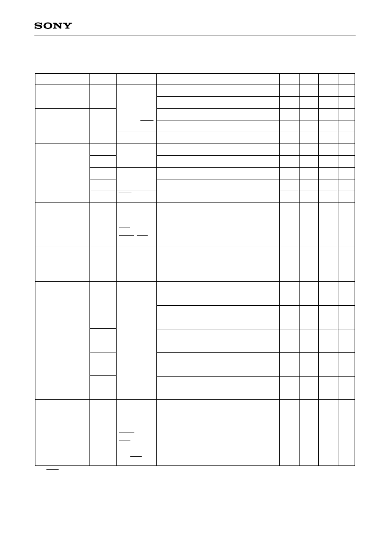
– 14 –
CXP80712B/80716B/80720B/80724B
V
DD
= 4.5V, I
OH
= –0.5mA
V
DD
= 4.5V, I
OH
= –1.2mA
V
DD
= 4.5V, I
OL
= 1.8mA
V
DD
= 4.5V, I
OL
= 3.6mA
V
DD
= 4.5V, I
OL
= 12.0mA
V
DD
= 5.5V, V
IH
= 5.5V
V
DD
= 5.5V, V
IL
= 0.4V
V
DD
= 5.5V, V
IH
= 5.5V
High level
output voltage
4.0
3.5
0.5
–0.5
0.1
–0.1
–1.5
V
V
V
V
V
μA
μA
μA
μA
μA
μA
μA
PD, PH
PA to PD,
PE2 to PE7,
PF4 to PF7,
PH (V
OL
only)
PI1 to PI7
PJ, SO0, SCK0
EXTAL
TEX
RST
1
Item
Symbol
Pins
Conditions
Min.
Clock 1MHz
0V other than the measured pins
V
DD
I
DD1
I
IZ
I
LOH
I
DDS1
I
DD2
I
DDS2
I
DDS3
C
IN
V
OH
V
OL
I
IHE
I
ILE
I
IHT
I
ILT
I
ILR
Low level
output voltage
Input current
Typ.
0.4
0.6
1.5
40
–40
10
–10
–400
±10
50
Max. Unit
DC Characteristics
Electrical Characteristics
(Ta = –20 to +75°C, Vss = 0V)
1
RST pin specifies the input current when the pull-up resistor is selected, and specifies leakage current
when no resistance is selected.
2
When entire output pins are open.
3
When setting upper 2 bits (CPU clock selection) of clock control register (CLC: 00FE
H
) to "00" and
operating in high speed mode (1/2 frequency dividing clock).
Supply current
2
Input capacity
V
DD
= 5.5V,
V
IL
= 0.4V
V
DD
= 5.5V,
V
I
= 0, 5.5V
V
DD
= 5.5V
V
OH
= 12V
I/O leakage
current
Open drain
output leakage
current (N-CH
Tr off state)
PA to PG,
PI, PJ, MP
AN0 to AN3,
CS0, SI0, SO0
SCK0, RST
1
PH
20
1.1
35
7
10
45
8
100
30
10
20
mA
mA
μA
μA
μA
pF
PC, PD,
PE0 to 1,
PF0 to 3, PG,
PI, PJ, AN,
SCK0, SI0,
CS0, EXTAL,
XTAL, TEX,
TX, RST, MP
16MHz crystal oscillation
(C
1
= C
2
= 15pF), V
DD
= 5.5V
16MHz crystal oscillation
(C
1
= C
2
= 15pF), V
DD
= 5.5V, SLEEP mode
32kHz crystal oscillation
(C
1
= C
2
= 47pF), V
DD
= 3.3V
32kHz crystal oscillation
(C
1
= C
2
= 47pF), V
DD
= 3.3V, SLEEP mode
V
DD
= 5.5V, STOP mode (termination of
32kHz and 16MHz crystal oscillation)
相關(guān)PDF資料 |
PDF描述 |
|---|---|
| CXP80720B | CMOS 8-bit Single Chip Microcomputer |
| CXP80732A | CMOS 8-bit Single Chip Microcomputer |
| CXP80740A | CMOS 8-bit Single Chip Microcomputer |
| CXP80732AQ | 8-BIT MICROCONTROLLER |
| CXP80732AR | 8-BIT MICROCONTROLLER |
相關(guān)代理商/技術(shù)參數(shù) |
參數(shù)描述 |
|---|---|
| CXP80716BQ | 制造商:未知廠家 制造商全稱:未知廠家 功能描述:8-Bit Microcontroller |
| CXP80716BR | 制造商:未知廠家 制造商全稱:未知廠家 功能描述:8-Bit Microcontroller |
| CXP80720A | 制造商:SONY 制造商全稱:Sony Corporation 功能描述:CMOS 8-bit Single Chip Microcomputer |
| CXP80720AQ | 制造商:未知廠家 制造商全稱:未知廠家 功能描述:8-Bit Microcontroller |
| CXP80720AR | 制造商:未知廠家 制造商全稱:未知廠家 功能描述:8-Bit Microcontroller |
發(fā)布緊急采購,3分鐘左右您將得到回復(fù)。