- 您現(xiàn)在的位置:買賣IC網(wǎng) > PDF目錄378472 > CXG1096FN (Sony Corporation) Power Amplifier/Antenna Switch + Low Noise Down Conversion Mixer for PHS PDF資料下載
參數(shù)資料
| 型號: | CXG1096FN |
| 廠商: | Sony Corporation |
| 英文描述: | Power Amplifier/Antenna Switch + Low Noise Down Conversion Mixer for PHS |
| 中文描述: | 功率放大器/天線開關低噪聲下變頻混頻器的小靈通 |
| 文件頁數(shù): | 3/7頁 |
| 文件大小: | 121K |
| 代理商: | CXG1096FN |
– 3 –
CXG1096FN
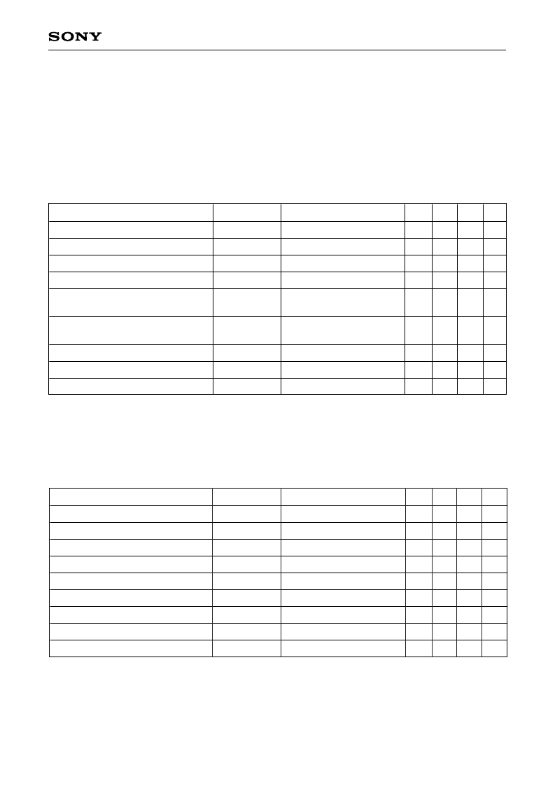
2. Antenna Switch Receiver Block + Low Noise Down Conversion Mixer Block
These specifications are common to the ANT1 reception and ANT2 reception.
Unless otherwise specified: V
DD
= 3V, RF1 = 1.90GHz/–35dBm, LO = 1.66GHz/–15dBm
When ANT1 reception: V
CTL
1 = 0V, V
CTL
2 = 3V
When ANT2 reception: V
CTL
1 = 3V, V
CTL
2 = 0V
Electrical Characteristics
These specifications are when the Sony's recommended evaluation board shown on page 6 is used.
1. Power Amplifier Block + Antenna Switch Transmitter Block
These specifications are common to the ANT1 transmission and ANT2 transmission.
Unless otherwise specified: V
DD
= 3V, I
DD
= 150mA, P
OUT
= 20.2dBm, f = 1.9GHz
When ANT1 transmission: V
CTL
1 = 3V, V
CTL
2 = 0V
When ANT2 transmission: V
CTL
1 = 0V, V
CTL
2 = 3V
Current consumption
Gate voltage adjustment value
Output power
Power gain
Adjacent channel leak power ratio
(600 ± 100kHz)
Adjacent channel leak power ratio
(900 ± 100kHz)
Occupied bandwidth
2nd-order harmonic level
3rd-order harmonic level
Item
I
DD
V
GG
P
OUT
G
P
ACPR600kHz
ACPR900kHz
OBW
—
—
Symbol
0.04
20.2
36
Min.
150
40
–63
–70
250
Typ.
0.6
–55
–60
275
–25
–25
Max.
mA
V
dBm
dB
dBc
dBc
kHz
dBc
dBc
Unit
Measured with the ANT pin
Measured with the ANT pin
Measured with the ANT pin
Measured with the ANT pin
Measured with the ANT pin
Measured with the ANT pin
Measurement conditions
Item
Symbol
Min. Typ. Max. Unit
Measurement conditions
(Ta = 25°C)
Current consumption
Conversion gain
Noise figure
Input IP3
Image suppression ratio
1/2 IF suppression ratio
2
×
LO–IF suppression ratio
2
×
LO+IF suppression ratio
LO to ANT leak
I
DD
G
C
NF
IIP3
IMR
1/2IFR
—
—
P
LK
17
–17
25
41
39
34
5.5
19.5
4.4
–12
40
47
45
65
–50
7.5
5.5
–40
mA
dB
dB
dBm
dBc
dBc
dBc
dBc
dBm
When no signal
When a small signal
When a small signal
1
RF2 = 1.42GHz/–35dBm
RF2 = 1.78GHz/–35dBm
RF2 = 3.08GHz/–35dBm
RF2 = 3.56GHz/–35dBm
(Ta = 25°C)
1
Conversion from IM3 compression ratio during FR1 = 1.9000GHz/–35dBm and FR2 = 1.9006GHz/–35dBm input.
相關PDF資料 |
PDF描述 |
|---|---|
| CXG1097EN | Low Noise Amplifier with Bypass Switch/Mixer |
| CXG1101TN | SP3T Antenna Switch for TDMA800/1900/AMPS800 Triple Mode Application |
| CXG1121TN | SP4T GSM/GPRS Dual-Band Antenna Switch + Logic |
| CXG1173UR | High Power SPDT Switch with Logic Control |
| CXK581000AYM-55SL | 131072-word x 8-bit High Speed CMOS Static RAM |
相關代理商/技術參數(shù) |
參數(shù)描述 |
|---|---|
| CXG1097EN | 制造商:SONY 制造商全稱:Sony Corporation 功能描述:Low Noise Amplifier with Bypass Switch/Mixer |
| CXG1100TN | 制造商:未知廠家 制造商全稱:未知廠家 功能描述:Wideband Multifunction Reception System GaAs MMIC Completely Covers GPS and CDMA |
| CXG1101TN | 制造商:SONY 制造商全稱:Sony Corporation 功能描述:SP3T Antenna Switch for TDMA800/1900/AMPS800 Triple Mode Application |
| CXG1104TN | 制造商:SONY 制造商全稱:Sony Corporation 功能描述:High Power SPDT Switch with Logic Control |
| CXG1106EN | 制造商:未知廠家 制造商全稱:未知廠家 功能描述:High Power 2x4 Antenna Switch MMIC with Integrated Control Logic |
發(fā)布緊急采購,3分鐘左右您將得到回復。