- 您現(xiàn)在的位置:買賣IC網(wǎng) > PDF目錄378985 > CXD3503R (Sony Corporation) Color Shading Correction IC for Liquid Crystal Projectors PDF資料下載
參數(shù)資料
| 型號: | CXD3503R |
| 廠商: | Sony Corporation |
| 英文描述: | Color Shading Correction IC for Liquid Crystal Projectors |
| 中文描述: | 彩色陰影校正集成電路液晶投影儀 |
| 文件頁數(shù): | 11/19頁 |
| 文件大小: | 175K |
| 代理商: | CXD3503R |
– 11 –
CXD3503R
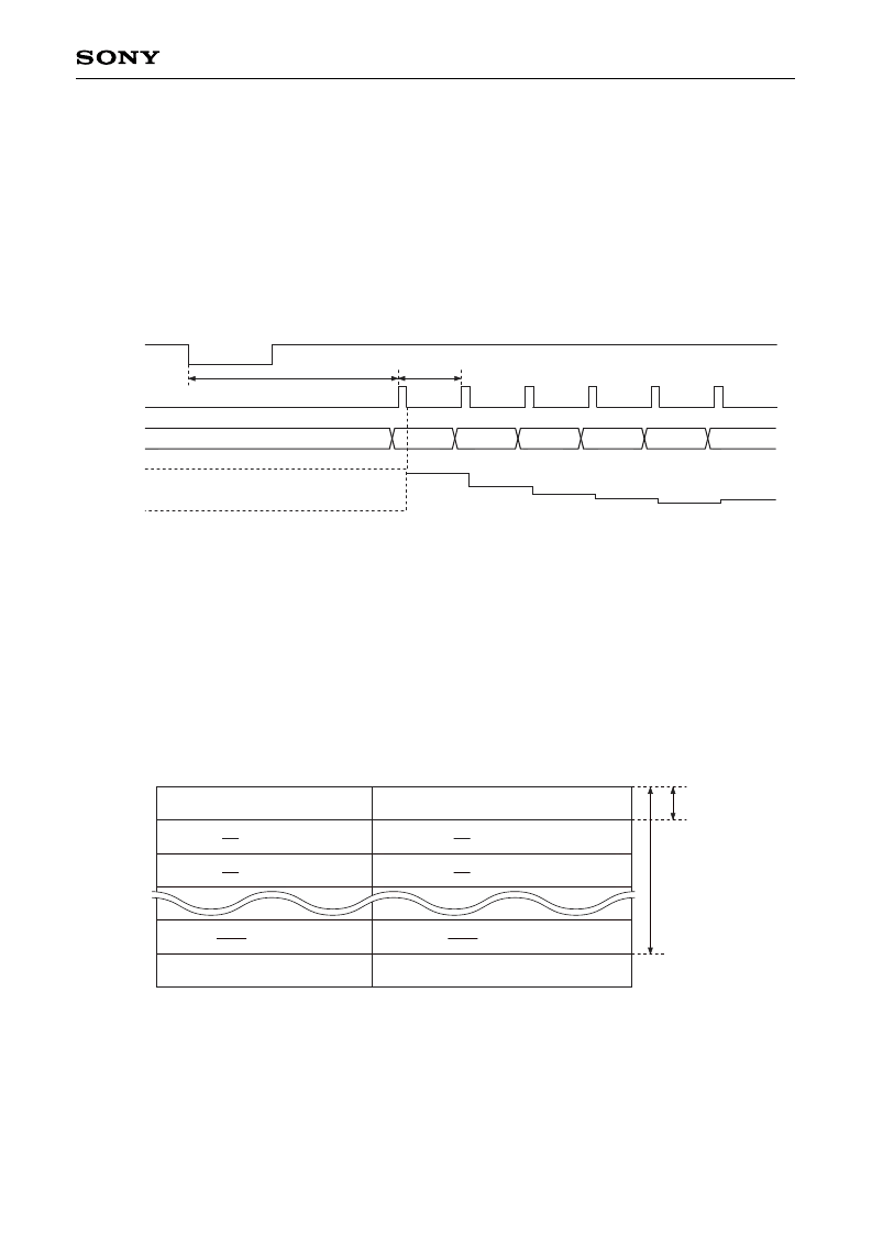
Description of Output Correction Signal Operation
Horizontal direction
The correction data set in the SRAM by serial transfer is arithmetically processed inside the IC to determine
the output position corresponding to the value set by serial register HP7 to 0 using the front edge of HSYNC as
the reference. Interpolation is not performed for the horizontal direction, and interpolated data is output at the
cycle set by serial register HINT7 to 0 for the vertical direction. In addition, the maximum amplitude of the
correction signal output voltage is determined by VRH (Pin 44) and VRL (Pin 40). The internal DAC outputs at
the resistive potential division (VRH to VRL: 213
typ.), so be sure to input to VRH and VRL via buffers having
current capacity.
Set by HINT7 to 0
Set by HP7 to 0
HSYNC
DACKO/I
DOUT
VRH
VRL
DACO
The internally generated digital data DOUT is input to the internal D/A converter, latched by the D/A converter
clock input from DACKI, and output from DACO2, 1 and 0 as an analog signal.
Note)
If edges remain, these level differences may appear as vertical stripes. Therefore, when using this as a
correction signal, be sure to eliminate the edges using an LPF, etc. before input to the CXA2111R or
CXA2112R.
Vertical direction
The vertical correction points set in the SRAM are arithmetically processed inside the IC to output interpolated
data for the lines other than correction points.
Vertical correction point interval
Set by VINT4 to 0 and ANM5 to 0
Assuming ANM5 to 0 = a,
a' = VINT
×
a
fm, n + a
2(fm
+ 1
, n – fm, n)
fm, n +
aa
+ 1
, n – fm, n)
fm
+ 1
, n
fm, n
fm, n + a
1(fm
+ 1
, n – fm, n)
fm, n
+ 1
+ a
2(fm
+ 1
, n
+ 1
– fm, n
+ 1
)
fm, n
+ 1
+
aa
+ 1
, n
+ 1
– fm, n
+ 1
)
fm
+ 1
, n
+ 1
fm
+ 1
, n
fm, n
+ 1
+ a
1(fm
+ 1
, n
+ 1
– fm, n
+ 1
)
m
n
n + 1
VINT line(s)
a' lines
fm, n: Correction data for point (m, n)
m + 1
相關(guān)PDF資料 |
PDF描述 |
|---|---|
| CXD3504R | Selective Delay Line For LCD(用于LCD的可選擇延遲線) |
| CXD3508ATQ | LCD Interface IC |
| CXD3508BTQ | LCD Interface IC |
| CXD3508TQ | LCD Interface IC |
| CXD3511Q | Digital Signal Driver/Timing Generator |
相關(guān)代理商/技術(shù)參數(shù) |
參數(shù)描述 |
|---|---|
| CXD3504R | 制造商:SONY 制造商全稱:Sony Corporation 功能描述:Color Shading Correction IC for Liquid Crystal Projectors |
| CXD3508ATQ | 制造商:SONY 制造商全稱:Sony Corporation 功能描述:LCD Interface IC |
| CXD3508BTQ | 制造商:SONY 制造商全稱:Sony Corporation 功能描述:LCD Interface IC |
| CXD3508TQ | 制造商:SONY 制造商全稱:Sony Corporation 功能描述:LCD Interface IC |
| CXD3511 | 制造商:SONY 制造商全稱:Sony Corporation 功能描述:Digital Signal Driver/Timing Generator |
發(fā)布緊急采購,3分鐘左右您將得到回復(fù)。