- 您現(xiàn)在的位置:買賣IC網(wǎng) > PDF目錄352822 > CS5159GD16 Analog IC PDF資料下載
參數(shù)資料
| 型號: | CS5159GD16 |
| 英文描述: | Analog IC |
| 中文描述: | 模擬IC |
| 文件頁數(shù): | 4/16頁 |
| 文件大小: | 197K |
| 代理商: | CS5159GD16 |
CS5151H
http://onsemi.com
12
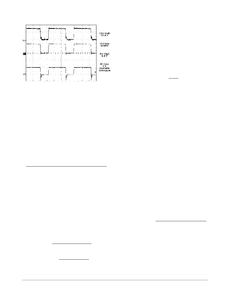
Figure 17. CS5151H Gate Drive Waveforms Depicting
Rail to Rail Swing
M 1.00
s
M1 = VGATE – 5.0 VIN
Channel 3 = VGATE
Channel 2– Inductor Switching Node
The most important aspect of MOSFET performance is
RDSON, which effects regulator efficiency and MOSFET
thermal management requirements.
The power dissipated by the MOSFET and the Schottky
diode may be estimated as follows;
Switching MOSFET:
Power
+ ILOAD2
RDSON
duty cycle
Schottky diode:
Power
+ VFORWARD
ILOAD
(1
* duty cycle)
Duty Cycle =
VOUT ) VFORWARD
VIN ) VFORWARD * (ILOAD
RDSON OF SYNCH FET)
Off Time Capacitor (COFF)
The COFF timing capacitor sets the regulator off time:
TOFF + COFF
4848.5
When the VFFB pin is less than 1.0 V, the current charging
the COFF capacitor is reduced. The extended off time can be
calculated as follows:
TOFF + COFF
24, 242.5
Off time will be determined by either the TOFF time, or the
time out timer, whichever is longer.
The preceding equations for duty cycle can also be used
to calculate the regulator switching frequency and select the
COFF timing capacitor:
COFF +
Perioid
(1
* duty cycle)
4848.5
where:
Period
+
1
switching frequency
“Droop” Resistor for Adaptive Voltage Positioning
Adaptive voltage positioning is used to reduce output
voltage excursions during abrupt changes in load current.
Regulator output voltage is offset +40 mV when the
regulator is unloaded, and –40 mV at full load. This results
in increased margin before encountering minimum and
maximum transient voltage limits, allowing use of less
capacitance on the regulator output (see Figure 9).
To implement adaptive voltage positioning, a “droop”
resistor must be connected between the output inductor and
output capacitors and load. This is normally implemented by
a PC board trace of the following value:
RDROOP +
80 mV
IMAX
Adaptive voltage positioning can be disabled for
improved DC regulation by connecting the VFB pin directly
to the load using a separate, non–load current carrying
circuit trace.
Input and Output Capacitors
These components must be selected and placed carefully
to yield optimal results. Capacitors should be chosen to
provide acceptable ripple on the input supply lines and
regulator output voltage. Key specifications for input
capacitors are their ripple rating, while ESR is important for
output capacitors. For best transient response, a combination
of low value/high frequency and bulk capacitors placed
close to the load will be required.
Output Inductor
The inductor should be selected based on its inductance,
current capability, and DC resistance. Increasing the
inductor value will decrease output voltage ripple, but
degrade transient response.
THERMAL MANAGEMENT
Thermal Considerations for Power
MOSFETs and Diodes
In order to maintain good reliability, the junction
temperature of the semiconductor components should be
kept to a maximum of 150
°C or lower. The thermal
impedance (junction to ambient) required to meet this
requirement can be calculated as follows:
Thermal Impedance
+
TJUNCTION(MAX) * TAMBIENT
Power
A heatsink may be added to TO–220 components to
reduce their thermal impedance. A number of PC board
layout techniques such as thermal vias and additional copper
foil area can be used to improve the power handling
capability of surface mount components.
相關PDF資料 |
PDF描述 |
|---|---|
| CS5159GDR16 | Analog IC |
| CS7311-4 | Optoelectronic |
| CS7311H4H | Optoelectronic |
| CS7321-4 | Optoelectronic |
| CS7331-4 | Optoelectronic |
相關代理商/技術參數(shù) |
參數(shù)描述 |
|---|---|
| CS-516003 | 制造商:未知廠家 制造商全稱:未知廠家 功能描述:Analog Attenuator |
| CS5160GD | 制造商:Rochester Electronics LLC 功能描述:- Bulk |
| CS5160GD16 | 制造商:Rochester Electronics LLC 功能描述:- Bulk |
| CS5160GDR16 | 制造商:Rochester Electronics LLC 功能描述:- Bulk |
| CS5161GD16 | 制造商:ON Semiconductor 功能描述: |
發(fā)布緊急采購,3分鐘左右您將得到回復。