- 您現(xiàn)在的位置:買賣IC網(wǎng) > PDF目錄352821 > CS51414GDR8 SMPS Controller PDF資料下載
參數(shù)資料
| 型號: | CS51414GDR8 |
| 英文描述: | SMPS Controller |
| 中文描述: | 開關電源控制器 |
| 文件頁數(shù): | 14/16頁 |
| 文件大小: | 489K |
| 代理商: | CS51414GDR8 |
CS51411, CS51412, CS51413, CS51414
http://onsemi.com
7
frequency foldback feature is disabled during the sync
mode.
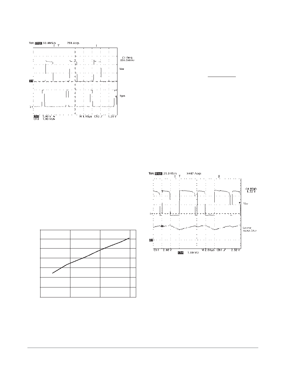
Figure 4. A CS51411 Buck Regulator is Synced by an
External 350 kHz Pulse Signal
Power Switch and Current Limit
The collector of the built–in NPN power switch is
connected to the VIN pin, and the emitter to the VSW pin.
When the switch turns on, the VSW voltage is equal to the
VIN minus switch Saturation Voltage. In the buck regulator,
the VSW voltage swings to one diode drop below ground
when the power switch turns off, and the inductor current is
commutated to the catch diode. Due to the presence of high
pulsed current, the traces connecting the VSW pin, inductor
and diode should be kept as short as possible to minimize the
noise and radiation. For the same reason, the input capacitor
should be placed close to the VIN pin and the anode of the
diode.
The saturation voltage of the power switch is dependent
on the switching current, as shown in Figure 5.
Figure 5. The Saturation Voltage of the Power Switch
Increases with the Conducting Current
0
0.5
1.0
1.5
Switching Current (A)
V
IN
–
V
SW
(V)
0
0.1
0.2
0.3
0.4
0.5
0.6
0.7
Members of the CS5141X family contain pulse–by–pulse
current limiting to protect the power switch and external
components. When the peak of the switching current reaches
the Current Limit, the power switch turns off after the
Current Limit Delay. The switch will not turn on until the
next switching cycle. The current limit threshold is
independent of switching duty cycle. The maximum load
current, given by the following formula under continuous
conduction mode, is less than the Current Limit due to the
ripple current.
IO(MAX) + ILIM *
VO(VIN * VO)
2(L)(VIN)(fs)
where:
fS = switching frequency,
ILIM = current limit threshold,
VO = output voltage,
VIN = input voltage,
L = inductor value.
When the regulator runs under current limit, the
subharmonic
oscillation
may
cause
low
frequency
oscillation, as shown in Figure 6. Similar to current mode
control, this oscillation occurs at the duty cycle greater than
50% and can be alleviated by using a larger inductor value.
The current limit threshold is reduced to Foldback Current
when the FB pin falls below Foldback Threshold. This
feature protects the IC and external components under the
power up or over–load conditions.
Figure 6. The Regulator in Current Limit
BOOST Pin
The BOOST pin provides base driving current for the
power switch. A voltage higher than VIN provides required
headroom to turn on the power switch. This in turn reduces
IC power dissipation and improves overall system
efficiency. The BOOST pin can be connected to an external
boost–strapping circuit which typically uses a 0.1
F capacitor
and a 1N914 or 1N4148 diode, as shown in Figure 1. When the
power switch is turned on, the voltage on the BOOST pin is
equal to
VBOOST + VIN ) VO * VF
where:
相關PDF資料 |
PDF描述 |
|---|---|
| CS-514-2DW18 | 2-Channel Disk Read/Write Circuit |
| CS-514-2RDW18 | 2-Channel Disk Read/Write Circuit |
| CS-514-4DW24 | 4-Channel Disk/Tape Read/Write Circuit |
| CS-514-6DW28 | 6-Channel Read/Write Circuit |
| CS-514-6FN28 | 6-Channel Read/Write Circuit |
相關代理商/技術參數(shù) |
參數(shù)描述 |
|---|---|
| CS51414GDR8G | 功能描述:直流/直流開關調(diào)節(jié)器 1.5A Low Voltage Buck RoHS:否 制造商:International Rectifier 最大輸入電壓:21 V 開關頻率:1.5 MHz 輸出電壓:0.5 V to 0.86 V 輸出電流:4 A 輸出端數(shù)量: 最大工作溫度: 安裝風格:SMD/SMT 封裝 / 箱體:PQFN 4 x 5 |
| CS51414GMNR2G | 功能描述:直流/直流開關調(diào)節(jié)器 1.5A 520kHz BUCK REG LOW VOLTAGE RoHS:否 制造商:International Rectifier 最大輸入電壓:21 V 開關頻率:1.5 MHz 輸出電壓:0.5 V to 0.86 V 輸出電流:4 A 輸出端數(shù)量: 最大工作溫度: 安裝風格:SMD/SMT 封裝 / 箱體:PQFN 4 x 5 |
| CS5141X-EVM | 制造商:ON Semiconductor 功能描述:CS5141X Evaluation Board |
| CS-514-2DW18 | 制造商:未知廠家 制造商全稱:未知廠家 功能描述:2-Channel Disk Read/Write Circuit |
| CS-514-2RDW18 | 制造商:未知廠家 制造商全稱:未知廠家 功能描述:2-Channel Disk Read/Write Circuit |
發(fā)布緊急采購,3分鐘左右您將得到回復。