- 您現(xiàn)在的位置:買賣IC網(wǎng) > PDF目錄169689 > CNY17-2 (VISHAY INTERTECHNOLOGY INC) 1 CHANNEL TRANSISTOR OUTPUT OPTOCOUPLER PDF資料下載
參數(shù)資料
| 型號: | CNY17-2 |
| 廠商: | VISHAY INTERTECHNOLOGY INC |
| 元件分類: | 光電耦合器 |
| 英文描述: | 1 CHANNEL TRANSISTOR OUTPUT OPTOCOUPLER |
| 封裝: | DIP-6 |
| 文件頁數(shù): | 1/4頁 |
| 文件大小: | 467K |
| 代理商: | CNY17-2 |
Document Number: 83606
www.vishay.com
Revision 17-August-01
2–68
FEATURES
High Current Transfer Ratio
CNY17-1, 40 to 80%
CNY17-2, 63 to 125%
CNY17-3, 100 to 200%
CNY17-4, 160 to 320%
Breakdown Voltage, 5300 VRMS
Field-Effect Stable by TRIOS—TRansparent
IOn Shield
Long Term Stability
Industry Standard Dual-in-Line Package
Underwriters Lab File #E52744
VDE #0884, Available with Option 1
DESCRIPTION
The CNY17 is an optically coupled pair consisting
of a Gallium Arsenide infrared emitting diode opti-
cally coupled to a silicon NPN phototransistor.
Signal information, including a DC level, can be trans-
mitted by the device while maintaining a high degree
of electrical isolation between input and output.
The CNY17 can be used to replace relays and trans-
formers in many digital interface applications, as well
as analog applications such as CRT modulation.
Maximum Ratings (TA=25°C)
Emitter
Reverse Voltage .............................................6.0 V
Forward Current .......................................... 60 mA
Surge Current (t
≤10 s)................................. 2.5 A
Power Dissipation......................................100 mW
Detector
Collector-Emitter Breakdown Voltage..............70 V
Emitter-Base Breakdown Voltage ...................7.0 V
Collector Current ......................................... 50 mA
Collector Current (t <1.0 ms)..................... 100 mA
Power Dissipation......................................150 mW
Package
Isolation Test Voltage (between emitter &
detector referred to climate DIN 50014,
part 2, Nov. 74) (t=1 sec)...................5300 VRMS
Creepage Distance .................................
≥7.0 mm
Clearance Distance.................................
≥7.0 mm
Isolation Thickness between
Emitter and Detector.............................
≥0.4 mm
Comparative Tracking Index per DIN IEC 112/
VDE0303, part 1 ........................................... 175
Isolation Resistance
VIO=500 V, TA=25°C.............................. ≥10
12
VIO=500 V, TA=100°C............................ ≥10
11
Storage Temperature...................–55°C to +150°C
Operating Temperature ...............–55°C to +100°C
Junction Temperature................................... 100°C
Soldering Temperature (max. 10 s, dip soldering:
distance to seating plane
≥1.5 mm) .........260°C
V
DE
Characteristics (TA=25°C)
Parameter
Symbol
Values
Unit
Condition
Emitter
Forward Voltage
VF
1.25
(
≤1.65)
V
IF = 60 mA
Breakdown Voltage
VBR
≥6.0
IR = 10 mA
Reverse Current
IR
0.01 (
≤10)
A
VR = 6.0 V
Capacitance
—
25
pF
VR=0 V, f=1.0 MHz
Thermal Resistance
Rthjamb
750
K/W
—
Detector
Capacitance
CCE
CCB
CEB
5.2
6.5
7.5
pF
VCE=5.0 V, f=1.0 MHz
VCB=5.0V,f=1.0MHz
VEB=5.0 V, f=1.0 MHz
Thermal Resistance
Rthjamb
500
K/W
—
Package
Collector-Emitter
Saturation Voltage
VCEsat
0.25 (
≤0.4)
V
IF =10 mA,
IC=2.5 mA
Coupling Capacitance
CC
0.6
pF
—
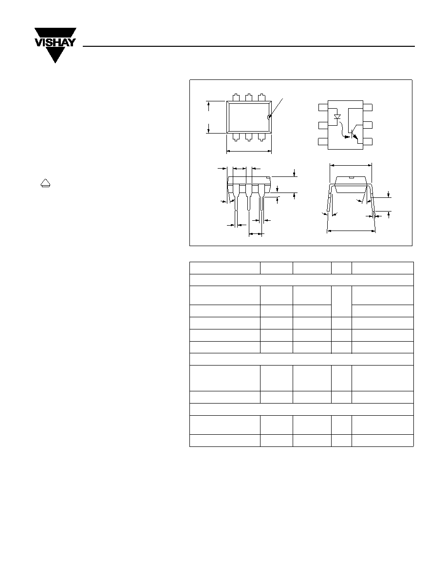
.010 (.25)
typ.
.114 (2.90)
.130 (3.0)
.130 (3.30)
.150 (3.81)
.031 (0.80) min.
.300 (7.62)
typ.
.031 (0.80)
.035 (0.90)
.100 (2.54) typ.
.039
(1.00)
Min.
.018 (0.45)
.022 (0.55)
.048 (1.22)
.022 (0.55)
.248 (6.30)
.256 (6.50)
.335 (8.50)
.343 (8.70)
pin one ID
6
5
4
1
2
3
18
°
3
°–9°
.300–.347
(7.62–8.81)
4
°
typ.
1
2
3
6
5
4
Base
Collector
Emitter
Anode
Cathode
NC
Dimensions in inches (mm)
CNY17
TRIOS Phototransistor
Optocoupler
相關(guān)PDF資料 |
PDF描述 |
|---|---|
| CNY17-3-300 | 1 CHANNEL TRANSISTOR OUTPUT OPTOCOUPLER |
| CNY17-3SR2 | 1 CHANNEL TRANSISTOR OUTPUT OPTOCOUPLER |
| CNY17-3X001 | 1 CHANNEL TRANSISTOR OUTPUT OPTOCOUPLER |
| CNY17-2X016 | 1 CHANNEL TRANSISTOR OUTPUT OPTOCOUPLER |
| CNY17F-3-X001 | 1 CHANNEL TRANSISTOR OUTPUT OPTOCOUPLER |
相關(guān)代理商/技術(shù)參數(shù) |
參數(shù)描述 |
|---|---|
| CNY17-2 | 功能描述:晶體管輸出光電耦合器 NPN Phototransistor RoHS:否 制造商:Vishay Semiconductors 輸入類型:DC 最大集電極/發(fā)射極電壓:70 V 最大集電極/發(fā)射極飽和電壓:0.4 V 絕緣電壓:5300 Vrms 電流傳遞比:100 % to 200 % 最大正向二極管電壓:1.65 V 最大輸入二極管電流:60 mA 最大集電極電流:100 mA 最大功率耗散:100 mW 最大工作溫度:+ 110 C 最小工作溫度:- 55 C 封裝 / 箱體:DIP-4 封裝:Bulk |
| CNY17-2 | 制造商:Vishay Semiconductors 功能描述:Optocoupler |
| CNY17-2.300 | 制造商:Fairchild Semiconductor Corporation 功能描述:OPTOCOUPLER TRANSISTOR O/P |
| CNY17-2.300 | 制造商:Fairchild Semiconductor Corporation 功能描述:OPTOCOuPLER ISOLATION VOLTAGE:5300V |
| CNY17-2.300 | 制造商:Fairchild Semiconductor Corporation 功能描述:OPTOCOUPLER TRANSISTOR O/P |
發(fā)布緊急采購,3分鐘左右您將得到回復(fù)。