- 您現(xiàn)在的位置:買賣IC網(wǎng) > PDF目錄298947 > CDCU877B (TT electronics Semelab Limited) 1.8-V PHASE LOCK LOOP CLOCK DRIVER PDF資料下載
參數(shù)資料
| 型號(hào): | CDCU877B |
| 廠商: | TT electronics Semelab Limited |
| 英文描述: | 1.8-V PHASE LOCK LOOP CLOCK DRIVER |
| 中文描述: | 的1.8 V鎖相環(huán)時(shí)鐘驅(qū)動(dòng)器 |
| 文件頁數(shù): | 14/17頁 |
| 文件大小: | 441K |
| 代理商: | CDCU877B |
www.ti.com
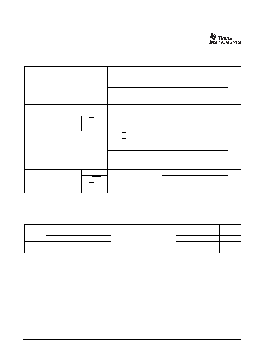
Electrical Characteristics
Timing Requirements
(1)
CDCU877B
1.8-V PHASE LOCK LOOP CLOCK DRIVER
SCAS801B – JUNE 2005 – REVISED JULY 2007
over recommended operating free-air temperature range (unless otherwise noted)
AVDD ,
PARAMETER
TEST CONDITIONS
MIN TYP(1)
MAX
UNIT
VDDQ
VIK
Input
II = 18 mA
1.7
-1.2
V
IOH = –100 μA
1.7 to 1.9
VDDQ – 0.2
VOH
High-level output voltage
V
IOH = –9 mA
1.7
1.1
IOL = 100 μA
0.1
VOL
Low-level output voltage
V
IOL = 9 mA
1.7
0.6
IO(DL)
Low-level output current, dissabled
VO(DL) = 100 mV, OE = L
1.7
100
μA
VOD
Differential output voltage(1)
1.7
0.5
V
CK, CK
1.9
±250
II
Input current
μA
OE, OS,
1.9
±10
FBIN, FBIN
IDD(LD)
Supply current, static (IDDQ + IADD)
CK and CK = L
1.9
500
μA
CK and CK = 270 MHz. All
outputs are open (not connected
1.9
115
to a PCB)
Supply current, dynamic (IDDQ + IADD)
IDD
All outputs are loaded with 2 pF
mA
(see Note (2) for CPD calculation)
1.9
215
and 120-
termination resistor
All outputs are loaded with 10 pF
1.9
235
and 120-
termination resistor
CK, CK
1.8
2
3
CI
Input capacitance
VI = VDD or GND
FBIN, FBIN
1.8
2
3
pF
CK, CK
1.8
0.25
CI(Δ)
Change in input current
VI = VDD or GND
FBIN, FBIN
1.8
0.25
(1)
VOD is the magnitude of the difference between the true and complimentary outputs. See Figure 9 for a definition.
(2)
Total IDD = IDDQ + IADD = fCK × CPD × VDDQ, solving for CPD = (IDDQ + IADD)/(fCK × VDDQ) where fCK is the input frequency, VDDQ is the
power supply, and CPD is the power dissipation capacitance.
over recommended operating free-air temperature range (unless otherwise noted) (see )
PARAMETER
TEST CONDITIONS
MIN
MAX
UNIT
Clock frequency (operating)(1)(2)
10
340
MHz
fCK
Clock frequency (application)(1)(3)
160
340
MHz
AVDD, VDD = 1.8 V ±0.1 V
tDC
Duty cycle, input clock
40%
60%
tL
Stabiliztion time (4)
12
μs
(1)
The PLL must be able to handle spread spectrum induced skew.
(2)
Operating clock frequency indicates a range over which the PLL must be able to lock, but in which it is not required to meet the other
timing parameters (used for low speed system debug).
(3)
Application clock frequency indicates a range over which the PLL must meet all timing parameters.
(4)
Stabilization time is the time required for the integrated PLL circuit to obtain phase lock of its feedback signal to its reference signal after
power up. During normal operation, the stabilization time is also the time required for the integrated PLL circuit to obtain phase lock of
its feedback signal to its reference signal when CK and CK go to a logic low state, enter the power-down mode and later return to active
operation. CK and CK may be left floating after they have been driven low for one complete clock cycle.
6
Submit Documentation Feedback
相關(guān)PDF資料 |
PDF描述 |
|---|---|
| CDEP85NP-1R4MB | 1 ELEMENT, 1.4 uH, GENERAL PURPOSE INDUCTOR, SMD |
| CDEP85NP-7R1MB | 1 ELEMENT, 7.1 uH, GENERAL PURPOSE INDUCTOR, SMD |
| CDG00 | DETECTOR DIODE |
| CDG22 | SILICON PLANAR BIASING DIODE |
| CDG23 | SILICON PLANAR BIASING DIODE |
相關(guān)代理商/技術(shù)參數(shù) |
參數(shù)描述 |
|---|---|
| CDCU877BZQLR | 功能描述:時(shí)鐘驅(qū)動(dòng)器及分配 1.8v PLL Clock Driver RoHS:否 制造商:Micrel 乘法/除法因子:1:4 輸出類型:Differential 最大輸出頻率:4.2 GHz 電源電壓-最大: 電源電壓-最小:5 V 最大工作溫度:+ 85 C 封裝 / 箱體:SOIC-8 封裝:Reel |
| CDCU877BZQLT | 功能描述:時(shí)鐘驅(qū)動(dòng)器及分配 1.8v PLL Clock Driver RoHS:否 制造商:Micrel 乘法/除法因子:1:4 輸出類型:Differential 最大輸出頻率:4.2 GHz 電源電壓-最大: 電源電壓-最小:5 V 最大工作溫度:+ 85 C 封裝 / 箱體:SOIC-8 封裝:Reel |
| CDCU877GQL | 制造商:TI 制造商全稱:Texas Instruments 功能描述:1.8V PHASE LOCK LOOP CLOCK DRIVER |
| CDCU877GQLR | 功能描述:時(shí)鐘驅(qū)動(dòng)器及分配 1.8v PLL Clock Driver RoHS:否 制造商:Micrel 乘法/除法因子:1:4 輸出類型:Differential 最大輸出頻率:4.2 GHz 電源電壓-最大: 電源電壓-最小:5 V 最大工作溫度:+ 85 C 封裝 / 箱體:SOIC-8 封裝:Reel |
| CDCU877GQLT | 功能描述:時(shí)鐘驅(qū)動(dòng)器及分配 1.8v PLL Clock Driver RoHS:否 制造商:Micrel 乘法/除法因子:1:4 輸出類型:Differential 最大輸出頻率:4.2 GHz 電源電壓-最大: 電源電壓-最小:5 V 最大工作溫度:+ 85 C 封裝 / 箱體:SOIC-8 封裝:Reel |
發(fā)布緊急采購,3分鐘左右您將得到回復(fù)。