- 您現(xiàn)在的位置:買賣IC網(wǎng) > PDF目錄366767 > CAT93C56YI-T2 2-Kb Microwire Serial CMOS EEPROM PDF資料下載
參數(shù)資料
| 型號: | CAT93C56YI-T2 |
| 英文描述: | 2-Kb Microwire Serial CMOS EEPROM |
| 中文描述: | 2 KB的Microwire串行EEPROM中的CMOS |
| 文件頁數(shù): | 5/18頁 |
| 文件大?。?/td> | 370K |
| 代理商: | CAT93C56YI-T2 |

CAT93C56, CAT93C57
Catalyst Semiconductor, Inc.
Characteristics subject to change without notice
5
Doc. No. MD-1088 Rev. P
POWER-UP TIMING
(1) (2)
Symbol
t
PUR
t
PUW
Parameter
Power-up to Read Operation
Power-up to Write Operation
Max
1
1
Units
ms
ms
Notes
:
(1) These parameters are tested initially and after a design or process change that affects the parameter according to appropriate
AEC-Q100 and JEDEC test methods.
(2) t
PUR
and t
PUW
are the delays required from the time V
CC
is stable until the specified operation can be initiated.
A.C. Test Conditions
Input Rise and Fall Times
Input Pulse Voltages
Timing Reference Voltages
Input Pulse Voltages
Timing Reference Voltages
Output Load
≤
50 ns
0.4V to 2.4V
0.8V, 2.0V
0.2V
CC
to 0.7V
CC
0.5V
CC
Current Source I
OLmax
/I
OHmax
; CL=100pF
4.5V
≤
V
CC
≤
5.5V
4.5V
≤
V
CC
≤
5.5V
1.8V
≤
V
CC
≤
4.5V
1.8V
≤
V
CC
≤
4.5V
DEVICE OPERATION
The CAT93C56/57 is a 2048-bit nonvolatile memory
intended for use with industry standard micropro-
cessors. The CAT93C56/57 can be organized as
either registers of 16 bits or 8 bits. When organized as
X16, seven 10-bit instructions for 93C57 or seven 11-
bit instructions for 93C56 control the reading, writing
and erase operations of the device. When organized
as X8, seven 11-bit instructions for 93C57 or seven
12-bit instructions for 93C56 control the reading,
writing and erase operations of the device. The
CAT93C56/57 operates on a single power supply and
will generate on chip, the high voltage required during
any write operation.
Instructions, addresses, and write data are clocked
into the DI pin on the rising edge of the clock (SK).
The DO pin is normally in a high impedance state
except when reading data from the device, or when
checking the ready/busy status after a write operation.
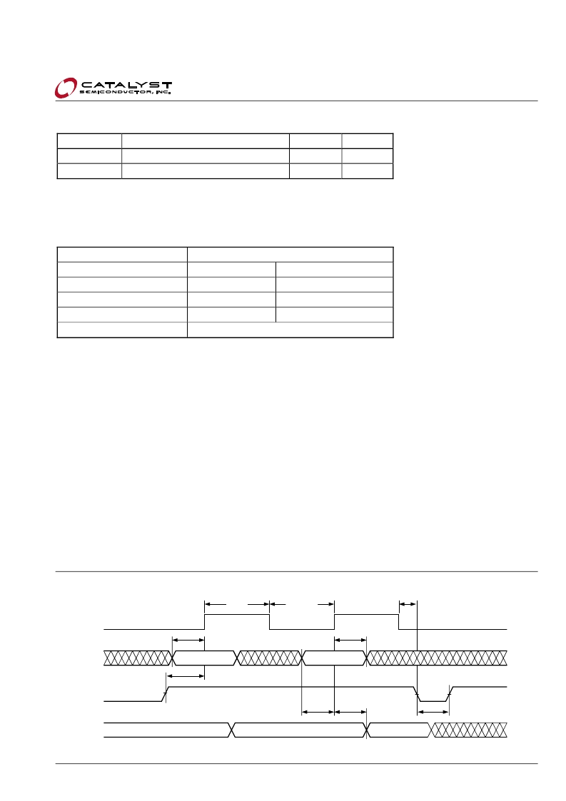
The serial communication protocol follows the timing
shown in Figure 1.
The ready/busy status can be determined after the start
of internal write cycle by selecting the device (CS high)
and polling the DO pin; DO low indicates that the write
operation is not completed, while DO high indicates that
the device is ready for the next instruction. If necessary,
the DO pin may be placed back into a high impedance
state during chip select by shifting a dummy “1” into the
DI pin. The DO pin will enter the high impedance state
on the rising edge of the clock (SK). Placing the DO pin
into the high impedance state is recommended in
applications where the DI pin and the DO pin are to be
tied together to form a common DI/O pin.
Figure 1. Sychronous Data Timing
SK
DI
CS
DO
tDIS
tPD0,tPD1
tCSMIN
tCSS
tDIS
tDIH
tSKHI
tCSH
VALID
VALID
DATA VALID
tSKLOW
相關(guān)PDF資料 |
PDF描述 |
|---|---|
| CAT93C56YI-T3 | 2-Kb Microwire Serial CMOS EEPROM |
| CAT93C56LI-GT2 | 2-Kb Microwire Serial CMOS EEPROM |
| CAT93C56LI-GT3 | 2-Kb Microwire Serial CMOS EEPROM |
| CAT93C56LI-T2 | 2-Kb Microwire Serial CMOS EEPROM |
| CAT93C56LI-T3 | 2-Kb Microwire Serial CMOS EEPROM |
相關(guān)代理商/技術(shù)參數(shù) |
參數(shù)描述 |
|---|---|
| CAT93C56YIT2E | 制造商:ONSEMI 制造商全稱:ON Semiconductor 功能描述:2-Kb Microwire Serial CMOS EEPROM |
| CAT93C56YIT3 | 制造商:ONSEMI 制造商全稱:ON Semiconductor 功能描述:2-Kb Microwire Serial CMOS EEPROM |
| CAT93C56YI-T3 | 制造商:CATALYST 制造商全稱:Catalyst Semiconductor 功能描述:2-Kb Microwire Serial CMOS EEPROM |
| CAT93C56YIT3E | 制造商:CATALYST 制造商全稱:Catalyst Semiconductor 功能描述:2K-Bit Microwire Serial EEPROM |
| CAT93C56YI-TE13 | 制造商:未知廠家 制造商全稱:未知廠家 功能描述:EEPROM |
發(fā)布緊急采購,3分鐘左右您將得到回復(fù)。