- 您現(xiàn)在的位置:買賣IC網(wǎng) > PDF目錄366750 > CAT64LC40JI-TE13 SPI Serial EEPROM PDF資料下載
參數(shù)資料
| 型號(hào): | CAT64LC40JI-TE13 |
| 英文描述: | SPI Serial EEPROM |
| 中文描述: | SPI串行EEPROM |
| 文件頁數(shù): | 8/11頁 |
| 文件大小: | 140K |
| 代理商: | CAT64LC40JI-TE13 |
8
CAT64LC10/20/40
Doc. No. 1021, Rev. A
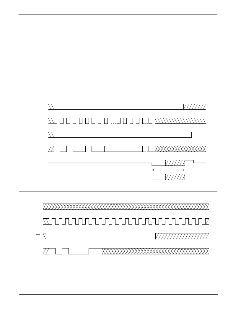
WRITE cycle. The RDY/
BSY
pin will output the
BUSY
status (LOW) one t
SV
after the rising edge of the 32nd
clock (the last data bit) and will stay LOW until the write
cycle is complete. Then it will output a logical “1” until the
next WRITE cycle. The RDY/
BSY
output is not affected
by the input of
CS
.
An alternative to get RDY/
BSY
status is from the DO pin.
During a write cycle, asserting a LOW input to the
CS
pin
will cause the DO pin to output the RDY/
BSY
status.
Bringing
CS
HIGH will bring the DO pin back to a high
impedance state again. After the device has completed
a WRITE cycle, the DO pin will output a logical “1” when
the device is deselected. The rising edge of the first “1”
input on the DI pin will reset DO back to the high
impedance state again.
The WRITE operation can be halted anywhere in the
operation by the RESET input. If a RESET pulse occurs
during a WRITE operation, the device will abort the
operation and output a READY status.
NOTE: Data may be corrupted if a RESET occurs while
the device is
BUSY
. If the reset occurs before the
BUSY
period, no writing will be initiated. However, if RESET
occurs after the
BUSY
period, new data will have been
written over the old data.
Figure 6. RESET During
BUSY
Instruction Timing
Figure 7. EWEN Instruction Timing
5064 FHD F09
* Please check instruction set table for address
SK
DI
CS
DO
RESET
1
0
1
0
0
1
0
0
ADDRESS*
D15
D0
tWR
RDY/
BUSY
SK
DI
CS
DO
RESET
1
0
1
0
0
0
1
1
HIGH-Z
HIGH
RDY/
BUSY
相關(guān)PDF資料 |
PDF描述 |
|---|---|
| CAT64LC40JI-TE7 | SPI Serial EEPROM |
| CAT64LC40J-TE13 | SPI Serial EEPROM |
| CAT64LC40J-TE7 | SPI Serial EEPROM |
| CAT64LC40P | SPI Serial EEPROM |
| CAT64LC40P-2.5 | SPI Serial EEPROM |
相關(guān)代理商/技術(shù)參數(shù) |
參數(shù)描述 |
|---|---|
| CAT64LC40JI-TE7 | 制造商:未知廠家 制造商全稱:未知廠家 功能描述:SPI Serial EEPROM |
| CAT64LC40J-T3 | 制造商:ONSEMI 制造商全稱:ON Semiconductor 功能描述:4 kb SPI Serial EEPROM |
| CAT64LC40JTE13 | 制造商:CATALYST 制造商全稱:Catalyst Semiconductor 功能描述:1K/2K/4K-Bit SPI Serial E2PROM |
| CAT64LC40J-TE13 | 制造商:未知廠家 制造商全稱:未知廠家 功能描述:SPI Serial EEPROM |
| CAT64LC40J-TE7 | 制造商:未知廠家 制造商全稱:未知廠家 功能描述:SPI Serial EEPROM |
發(fā)布緊急采購(gòu),3分鐘左右您將得到回復(fù)。