- 您現(xiàn)在的位置:買賣IC網 > PDF目錄366717 > CAT25C16AN-90T 16K-Bit CMOS PARALLEL EEPROM PDF資料下載
參數資料
| 型號: | CAT25C16AN-90T |
| 英文描述: | 16K-Bit CMOS PARALLEL EEPROM |
| 中文描述: | 16K的位CMOS并行的EEPROM |
| 文件頁數: | 3/10頁 |
| 文件大小: | 427K |
| 代理商: | CAT25C16AN-90T |
CAT28C16A
3
Doc. No. 1076, Rev. D
*COMMENT
Stresses above those listed under
“
Absolute Maximum
Ratings
”
may cause permanent damage to the device.
These are stress ratings only, and functional operation
of the device at these or any other conditions outside of
those listed in the operational sections of this specifica-
tion is not implied. Exposure to any absolute maximum
rating for extended periods may affect device perfor-
mance and reliability.
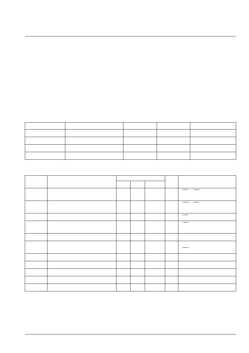
ABSOLUTE MAXIMUM RATINGS*
Temperature Under Bias .................
–
55
°
C to +125
°
C
Storage Temperature.......................
–
65
°
C to +150
°
C
Voltage on Any Pin with
Respect to Ground
(2)
...........
–
2.0V to +V
CC
+ 2.0V
V
CC
with Respect to Ground ...............
–
2.0V to +7.0V
Package Power Dissipation
Capability (Ta = 25
°
C)................................... 1.0W
Lead Soldering Temperature (10 secs) ............ 300
°
C
Output Short Circuit Current
(3)
........................ 100 mA
D.C. OPERATING CHARACTERISTICS
V
CC
= 5V
±
10%, unless otherwise specified.
Limits
Symbol
Parameter
Min
Typ
Max
Units
Test Conditions
I
CC
V
CC
Current (Operating, TTL)
35
mA
CE = OE = V
IL
,
f = 1/t
RC
min, All I/O
’
s Open
I
CCC(5)
V
CC
Current (Operating, CMOS)
25
mA
CE = OE = V
ILC
,
f = 1/t
RC
min, All I/O
’
s Open
I
SB
V
CC
Current (Standby, TTL)
1
mA
CE = V
IH
, All I/O
’
s Open
I
SBC(6)
V
CC
Current (Standby, CMOS)
100
μ
A
CE = V
IHC
,
All I/O
’
s Open
I
LI
Input Leakage Current
–
10
10
μ
A
μ
A
V
IN
= GND to V
CC
I
LO
Output Leakage Current
–
10
10
V
OUT
= GND to V
CC
,
CE = V
IH
V
IH(6)
High Level Input Voltage
2
V
CC
+0.3
V
V
IL(5)
Low Level Input Voltage
–
0.3
0.8
V
V
OH
High Level Output Voltage
2.4
V
I
OH
=
–
400
μ
A
V
OL
Low Level Output Voltage
0.4
V
I
OL
= 2.1mA
V
WI
Write Inhibit Voltage
3.0
V
RELIABILITY CHARACTERISTICS
Symbol
N
END(1, 7)
Parameter
Min
Max
Units
Endurance
100,000
Cycles/Byte
T
DR(1, 7)
Data Retention
100
Years
V
ZAP(1)
ESD Susceptibility
2000
Volts
I
LTH(1)(4)
Latch-Up
100
mA
Note:
(1) This parameter is tested initially and after a design or process change that affects the parameter.
(2) The minimum DC input voltage is
–
0.5V. During transitions, inputs may undershoot to
–
2.0V for periods of less than 20 ns. Maximum DC
voltage on output pins is V
CC
+0.5V, which may overshoot to V
CC
+2.0V for periods of less than 20 ns.
(3) Output shorted for no more than one second. No more than one output shorted at a time.
(4) Latch-up protection is provided for stresses up to 100mA on address and data pins from
–
1V to V
CC
+1V.
(5) V
ILC
=
–
0.3V to +0.3V.
(6) V
IHC
= V
CC
–
0.3V to V
CC
+0.3V.
(7) For the CAT28C16A-20, the minimum endurance is 10,000 cycles and the minimum data retention is 10 years.
相關PDF資料 |
PDF描述 |
|---|---|
| CAT25C16ANA-12T | 16K-Bit CMOS PARALLEL EEPROM |
| CAT25C16ANA-20T | 16K-Bit CMOS PARALLEL EEPROM |
| CAT25C16ANA-90T | 16K-Bit CMOS PARALLEL EEPROM |
| CAT25C16ANI-12T | 16K-Bit CMOS PARALLEL EEPROM |
| CAT25C16ANI-20T | 16K-Bit CMOS PARALLEL EEPROM |
相關代理商/技術參數 |
參數描述 |
|---|---|
| CAT25C16L | 功能描述:電可擦除可編程只讀存儲器 (2048x8) 16K RoHS:否 制造商:Atmel 存儲容量:2 Kbit 組織:256 B x 8 數據保留:100 yr 最大時鐘頻率:1000 KHz 最大工作電流:6 uA 工作電源電壓:1.7 V to 5.5 V 最大工作溫度:+ 85 C 安裝風格:SMD/SMT 封裝 / 箱體:SOIC-8 |
| CAT25C16L-1.8 | 功能描述:電可擦除可編程只讀存儲器 (2048x8) 16K RoHS:否 制造商:Atmel 存儲容量:2 Kbit 組織:256 B x 8 數據保留:100 yr 最大時鐘頻率:1000 KHz 最大工作電流:6 uA 工作電源電壓:1.7 V to 5.5 V 最大工作溫度:+ 85 C 安裝風格:SMD/SMT 封裝 / 箱體:SOIC-8 |
| CAT25C16LA | 功能描述:電可擦除可編程只讀存儲器 (2048x8) 16K RoHS:否 制造商:Atmel 存儲容量:2 Kbit 組織:256 B x 8 數據保留:100 yr 最大時鐘頻率:1000 KHz 最大工作電流:6 uA 工作電源電壓:1.7 V to 5.5 V 最大工作溫度:+ 85 C 安裝風格:SMD/SMT 封裝 / 箱體:SOIC-8 |
| CAT25C16LGI | 制造商:Rochester Electronics LLC 功能描述: 制造商:Catalyst Semiconductor 功能描述: |
| CAT25C16LI | 功能描述:電可擦除可編程只讀存儲器 (2048x8) 16K RoHS:否 制造商:Atmel 存儲容量:2 Kbit 組織:256 B x 8 數據保留:100 yr 最大時鐘頻率:1000 KHz 最大工作電流:6 uA 工作電源電壓:1.7 V to 5.5 V 最大工作溫度:+ 85 C 安裝風格:SMD/SMT 封裝 / 箱體:SOIC-8 |
發(fā)布緊急采購,3分鐘左右您將得到回復。