- 您現(xiàn)在的位置:買賣IC網(wǎng) > PDF目錄366705 > CAT25040PI The CAT24FC02 is a 2-kb Serial CMOS EEPROM internally organized as 256 words of 8 bits each PDF資料下載
參數(shù)資料
| 型號: | CAT25040PI |
| 元件分類: | DRAM |
| 英文描述: | The CAT24FC02 is a 2-kb Serial CMOS EEPROM internally organized as 256 words of 8 bits each |
| 中文描述: | 該CAT24FC02是一個2 KB的EEPROM的國內256個8位每字舉辦的串行CMOS |
| 文件頁數(shù): | 9/11頁 |
| 文件大?。?/td> | 73K |
| 代理商: | CAT25040PI |
9
CAT25010/20/40
Doc. No. 1006, Rev. L
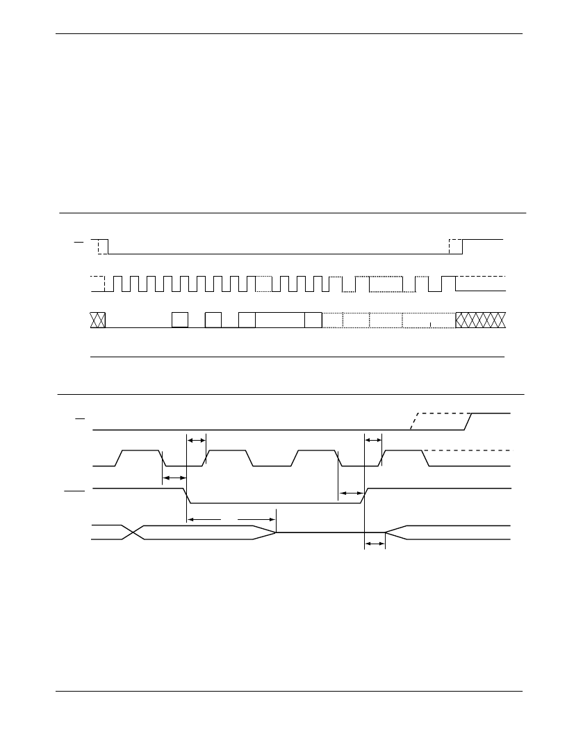
Figure 9.
HOLD
Timing
DESIGN CONSIDERATIONS
The CAT250140/20/40 powers up in a write disable
state and in a low power standby mode. A WREN
instruction must be issued to perform any writes to the
device after power up. Also,on power up
CS
should be
brought low to enter a ready state and receive an
instruction. After a successful byte/page write or status
register write, the CAT250140/20/40 goes into a write
disable mode.
CS
must be set high after the proper
number of clock cycles to start an internal write cycle.
Access to the array during an internal write cycle is
ignored and programming is continued. On power up,
Figure 8. Page Write Instruction Timing
Note: Dashed Line= mode (1, 1)
–
– – – –
*X=0 for 25010, 25020 ; X=A8 for 25040
Note: Dashed Line= mode (1, 1)
–
– – – –
CS
SCK
HOLD
SO
tCD
tHD
tHD
tCD
tLZ
tHZ
HIGH IMPEDANCE
SO is in a high impedance. If an invalid op code is
received, no data will be shifted into the CAT250140/
20/40, and the serial output pin (SO) will remain in a
high impedance state until the falling edge of
CS
is
detected again.
When powering down, the supply should be taken down
to 0V, so that the CAT250140/20/40 will be reset when
power is ramped back up. If this is not possible, then,
following a brown-out episode, the CAT250140/20/40
can be reset by refreshing the contents of the Status
Register (See Application Note AN10).
SK
SI
SO
0
0
0
0
0
X*
0
1
0
BYTE ADDRESS
Data
Byte 1
0
1
2
3
4
5
6
7
8
13
14
15 16-23
24-31
Data
Byte 2
Data
Byte 3
Data Byte N
7..1
CS
OPCODE
0
16+(N-1)x8-1..16+(N-1)x8 16+Nx8-1
DATA IN
HIGH IMPEDANCE
A7
A0
發(fā)布緊急采購,3分鐘左右您將得到回復。