- 您現(xiàn)在的位置:買賣IC網(wǎng) > PDF目錄298913 > CAT25010VE-1.8TE13 EEPROM PDF資料下載
參數(shù)資料
| 型號: | CAT25010VE-1.8TE13 |
| 元件分類: | EEPROM |
| 英文描述: | EEPROM |
| 中文描述: | EEPROM的 |
| 文件頁數(shù): | 5/10頁 |
| 文件大小: | 77K |
| 代理商: | CAT25010VE-1.8TE13 |

4
CAT25010/20/40
Doc. No. 1006, Rev. G
FUNCTIONAL DESCRIPTION
The CAT25010/20/40 supports the SPI bus data
transmission protocol. The synchronous Serial Peripheral
Interface (SPI) helps the CAT25010/20/40 to interface
directly with many of today’s popular microcontrollers.
The CAT25010/20/40 contains an 8-bit instruction
register. (The instruction set and the operation codes
are detailed in the instruction set table)
After the device is selected with
CS going low, the first
byte will be received. The part is accessed via the SI pin,
with data being clocked in on the rising edge of SCK.
The first byte contains one of the six op-codes that define
the operation to be performed.
PIN DESCRIPTION
SI: Serial Input
SI is the serial data input pin. This pin is used to input all
opcodes, byte addresses, and data to be written to the
CAT25010/20/40. Input data is latched on the rising
edge of the serial clock for SPI modes (0, 0 & 1, 1).
SO: Serial Output
SO is the serial data output pin. This pin is used to
transfer data out of the CAT25010/20/40. During a read
cycle, data is shifted out on the falling edge of the serial
Note:
(1) X=0 for 25010, 25020. X=A8 for 25040
(2) This parameter is tested initially and after a design or process change that affects the parameter.
(3) tPUR and tPUW are the delays required from the time VCC is stable until the specified operation can be initiated.
Power-Up Timing(2)(3)
Symbol
Parameter
Max.
Units
tPUR
Power-up to Read Operation
1
ms
tPUW
Power-up to Write Operation
1
ms
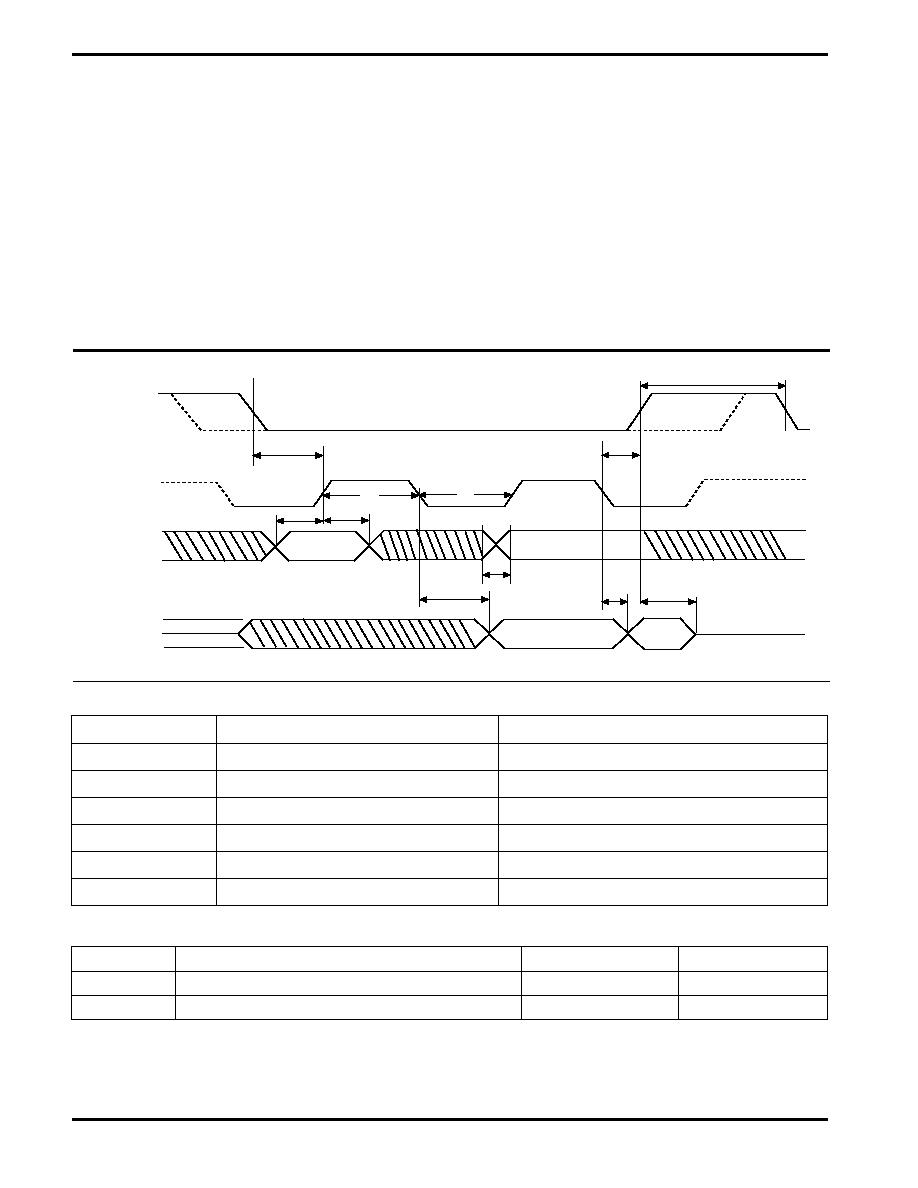
Figure 1. Sychronous Data Timing
VALID IN
VIH
VIL
tCSS
VIH
VIL
VIH
VIL
VOH
VOL
HI-Z
tSU
tH
tWH
tWL
tV
tCS
tCSH
tHO
tDIS
HI-Z
CS
SCK
SI
SO
tRI
tFI
Note: Dashed Line= mode (1, 1) – ––––
Instruction
Opcode
Operation
WREN
0000 0110
Enable Write Operations
WRDI
0000 0100
Disable Write Operations
RDSR
0000 0101
Read Status Register
WRSR
0000 0001
Write Status Register
READ
0000 X011(1)
Read Data from Memory
WRITE
0000 X010(1)
Write Data to Memory
INSTRUCTION SET
相關(guān)PDF資料 |
PDF描述 |
|---|---|
| CAT25010VE-TE13 | EEPROM |
| CAT25010VI-1.8 | EEPROM |
| CAT25010ZA-1.8TE13 | EEPROM |
| CAT25010ZA-TE13 | EEPROM |
| CAT25010ZE-1.8 | EEPROM |
相關(guān)代理商/技術(shù)參數(shù) |
參數(shù)描述 |
|---|---|
| CAT25010VE-G | 制造商:ON Semiconductor 功能描述: |
| CAT25010VE-GT3 | 制造商:Rochester Electronics LLC 功能描述: 制造商:ON Semiconductor 功能描述: |
| CAT25010VE-GT3D | 功能描述:電可擦除可編程只讀存儲器 1KB SPI SER CMOS 電可擦除可編程只讀存儲器 RoHS:否 制造商:Atmel 存儲容量:2 Kbit 組織:256 B x 8 數(shù)據(jù)保留:100 yr 最大時鐘頻率:1000 KHz 最大工作電流:6 uA 工作電源電壓:1.7 V to 5.5 V 最大工作溫度:+ 85 C 安裝風(fēng)格:SMD/SMT 封裝 / 箱體:SOIC-8 |
| CAT25010VGI | 制造商:Catalyst Semiconductor 功能描述: |
| CAT25010VGI-T3 | 制造商:Rochester Electronics LLC 功能描述: 制造商:Catalyst Semiconductor 功能描述: |
發(fā)布緊急采購,3分鐘左右您將得到回復(fù)。