- 您現(xiàn)在的位置:買賣IC網(wǎng) > PDF目錄210370 > BU-65142D2-320Q (DATA DEVICE CORP) 2 CHANNEL(S), 1M bps, MIL-STD-1553 CONTROLLER, CQIP78 PDF資料下載
參數(shù)資料
| 型號: | BU-65142D2-320Q |
| 廠商: | DATA DEVICE CORP |
| 元件分類: | 微控制器/微處理器 |
| 英文描述: | 2 CHANNEL(S), 1M bps, MIL-STD-1553 CONTROLLER, CQIP78 |
| 封裝: | 45.70 X 53.30 MM, 5.30 MM HEIGHT, CERAMIC, QIP-78 |
| 文件頁數(shù): | 15/28頁 |
| 文件大?。?/td> | 264K |
| 代理商: | BU-65142D2-320Q |
第1頁第2頁第3頁第4頁第5頁第6頁第7頁第8頁第9頁第10頁第11頁第12頁第13頁第14頁當前第15頁第16頁第17頁第18頁第19頁第20頁第21頁第22頁第23頁第24頁第25頁第26頁第27頁第28頁

22
Data Device Corporation
www.ddc-web.com
BU-65142 SERIES
V-01/03-0
SSBUSY
55
71
Subsystem Busy - input from the subsystem
used to control the busy bit in the status regis-
ter. If LOW when the status word is updated,
the busy bit will be set, if HIGH it will be
cleared. If the busy bit is set in the status reg-
ister, no data will be requested from the sub-
system in response to a transmit command.
On receive commands, data will be transferred
to the subsystem.
SSFLAG
53
72
Subsystem Flag-- input from the subsystem
used to control the subsystem flag bit in the
status register. If LOW when the status word
is updated, the subsystem flag will be set; if
HIGH it will be cleared.
FUNC-
TION
78-Pin
Flat-
Pack
DESCRIPTION
PACKAGE & PIN
TABLE 7. PIN FUNCTIONS (continued)
78-Pin
QIP
These pins are not used on this package.
Status Word Enable-- LOW level active output
signal present when the status word is
enabled on the parallel data bus.
N/C
STATEN
Low output to the primary side of the coupling
transformer that connects to the A channel of
the 1553 Bus.
TXDATA
A
Not connected.
N/C
Power supply return connection for the A
channel transceiver.
GND A
Input from the HIGH side of the primary side
of the coupling transformer that connects to
the A channel of the 1553 Bus.
RXDA-
TA A
Message Error--output signal that goes LOW
and stays LOW whenever there is a format or
word error with the received message over the
1553 Data Bus. Cleared by the next NGBT.
ME
_
41
_
78
43
77
45
76
47
75
49
74
73
51
PIN FUNCTION TABLE NOTES(TABLE 6) :
1. TEST 2
This pin provides the output of the BU-65142 BIT Comparison output.
It indicates the loop test results for every word transmitted by the BU-
65142. A test can be performed by actioning the RTU to transmit while
the test fixture opens the receiver lines to force an error condition. A
logic 1 (high) indicates the loop test passed. Normally this pin is left
open.
2. BUFENA
This pin is typically tied to DTACK, causing the BU-65142 to drive the
shared data bus only while DTACK is active. If desired BUFENA can
be grounded. The data will remain latched on the data bus pins for
18s from DTRSB and 3.5s for the last word of a message as the
device’s status word or BIT word is transferred to the BC
(STATEN or BITEN low). Once the STATUS or BIT Word transfer is
complete, the data bus will automatically again contain the last data
word. The BU-65142 will automatically switch the direction of the inter-
nal buffers during a transmit operation.
3. TEST 1
This test allows the user to force the active channel to transmit indef-
initely, in order to test the built in Watchdog Timer feature of the BU-
65142. When this pin is grounded and the active channel is stimulat-
ed with a valid transmit command, the BU-65142 will respond with a
status word and contiguous data (last data word loaded or STATUS
WORD if none is loaded) until the built-in time out occurs. Normally
this pin is left open or an optional pull-up can be used.
4. -VA and -VB are not connected (N/C) for BU-65142X3.
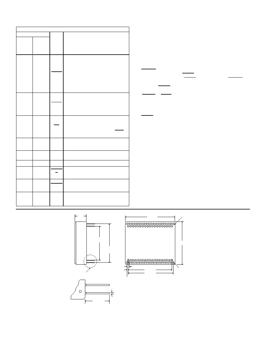
FIGURE 8. BU-65142D MECHANICAL OUTLINE (HI-REL RADIATION TOLERANT VERSION
(78-PIN CERAMIC QIP)
1.800 MAX
(46)
1.500
(38)
1.800 (46)
INDEX
DENOTES
PIN 1
2.100 MAX
(53)
1.900 (48)
0.210
MAX
(5.33)
0.100 TYP (2.54)
0.250 ±0.010
(6.35 ±0.25)
PIN NUMBERS FOR
REFERENCE ONLY
1.650
(42)
0.018 ±0.002 DIA TYP
(0.46 ±0.05)
59
20
40
78
60
21
41
1
2
SEE DETAIL "A"
0.050 TYP (1.27)
DETAIL "A"
NOTE: DIMENSIONS ARE IN INCHES (MM).
相關(guān)PDF資料 |
PDF描述 |
|---|---|
| BU-65142D2-340L | 2 CHANNEL(S), 1M bps, MIL-STD-1553 CONTROLLER, CQIP78 |
| BU-65142D2-390K | 2 CHANNEL(S), 1M bps, MIL-STD-1553 CONTROLLER, CQIP78 |
| BU-65142D2-450L | 2 CHANNEL(S), 1M bps, MIL-STD-1553 CONTROLLER, CQIP78 |
| BU-65142D3-120Y | 2 CHANNEL(S), 1M bps, MIL-STD-1553 CONTROLLER, CQIP78 |
| BU-65142D3-140Q | 2 CHANNEL(S), 1M bps, MIL-STD-1553 CONTROLLER, CQIP78 |
相關(guān)代理商/技術(shù)參數(shù) |
參數(shù)描述 |
|---|---|
| BU65170G0-100 | 制造商:未知廠家 制造商全稱:未知廠家 功能描述:Interface IC |
| BU65170G0-110 | 制造商:未知廠家 制造商全稱:未知廠家 功能描述:Interface IC |
| BU65170G0-120 | 制造商:未知廠家 制造商全稱:未知廠家 功能描述:Interface IC |
| BU65170G0-200 | 制造商:未知廠家 制造商全稱:未知廠家 功能描述:Interface IC |
| BU65170G0-300 | 制造商:未知廠家 制造商全稱:未知廠家 功能描述:Interface IC |
發(fā)布緊急采購,3分鐘左右您將得到回復。