- 您現(xiàn)在的位置:買賣IC網(wǎng) > PDF目錄256309 > BU-61582D0-290Z (DATA DEVICE CORP) 2 CHANNEL(S), 1M bps, MIL-STD-1553 CONTROLLER, CQIP70 PDF資料下載
參數(shù)資料
| 型號: | BU-61582D0-290Z |
| 廠商: | DATA DEVICE CORP |
| 元件分類: | 微控制器/微處理器 |
| 英文描述: | 2 CHANNEL(S), 1M bps, MIL-STD-1553 CONTROLLER, CQIP70 |
| 封裝: | CERAMIC, DIP-70 |
| 文件頁數(shù): | 25/48頁 |
| 文件大小: | 378K |
| 代理商: | BU-61582D0-290Z |
第1頁第2頁第3頁第4頁第5頁第6頁第7頁第8頁第9頁第10頁第11頁第12頁第13頁第14頁第15頁第16頁第17頁第18頁第19頁第20頁第21頁第22頁第23頁第24頁當前第25頁第26頁第27頁第28頁第29頁第30頁第31頁第32頁第33頁第34頁第35頁第36頁第37頁第38頁第39頁第40頁第41頁第42頁第43頁第44頁第45頁第46頁第47頁第48頁
31
Data Device Corporation
www.ddc-web.com
BU-61582
G-08/02-250
SELECT
MSB/LSB
MEM/REG
A15-A0
ADDRESS_LAT
SELECT
MSB/LSB
MEM/REG
A15-A0
(1)
(2)
(3)
(4)
(1)
(2)
(3)
(4)
(5)
t1
INTERNAL
VALUES
INPUT
SIGNALS
t2
t4
t5
t3
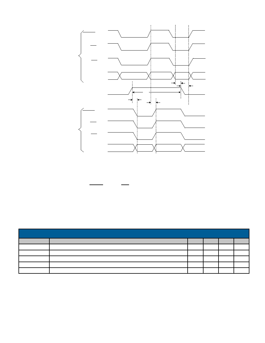
FIGURE 15. ADDRESS LATCH TIMING
Notes for FIGURE 15 and associated table.
1. Applicable to buffered mode only. Address SELECT AND MEM/REG latches are always transparent in the transparent mode of operation.
2. Latches are transparent when ADDR_LAT is high. Internal values do not update when ADDR_LAT is low.
3. MSB/LSB input signal is applicable to 8-bit mode only (16/8 input = logic “0”). MSB/LSB input is a “don’t care” for 16-bit operation.
ns
20
Input hold time following falling edge of ADDR_LAT
t5
ns
10
Input setup time prior to falling edge of ADDR_LAT
t4
ns
10
Propagation delay from external input signals to internal signals valid
t3
ns
10
ADDR_LAT high delay to internal signals valid
t2
ns
20
ADDR_LAT pulse width
t1
UNITS
MAX
TYP
MIN
DESCRIPTION
REF
TABLE FOR FIGURE 15. ADDRESS LATCH TIMING
發(fā)布緊急采購,3分鐘左右您將得到回復(fù)。