- 您現(xiàn)在的位置:買賣IC網(wǎng) > PDF目錄256340 > BU-61559F2-650K (DATA DEVICE CORP) 2 CHANNEL(S), 1M bps, MIL-STD-1553 CONTROLLER, CDFP78 PDF資料下載
參數(shù)資料
| 型號(hào): | BU-61559F2-650K |
| 廠商: | DATA DEVICE CORP |
| 元件分類: | 微控制器/微處理器 |
| 英文描述: | 2 CHANNEL(S), 1M bps, MIL-STD-1553 CONTROLLER, CDFP78 |
| 封裝: | 45.70 X 53.30 MM, 5.30 MM HEIGHT, CERAMIC, FP-78 |
| 文件頁(yè)數(shù): | 10/32頁(yè) |
| 文件大?。?/td> | 438K |
| 代理商: | BU-61559F2-650K |
第1頁(yè)第2頁(yè)第3頁(yè)第4頁(yè)第5頁(yè)第6頁(yè)第7頁(yè)第8頁(yè)第9頁(yè)當(dāng)前第10頁(yè)第11頁(yè)第12頁(yè)第13頁(yè)第14頁(yè)第15頁(yè)第16頁(yè)第17頁(yè)第18頁(yè)第19頁(yè)第20頁(yè)第21頁(yè)第22頁(yè)第23頁(yè)第24頁(yè)第25頁(yè)第26頁(yè)第27頁(yè)第28頁(yè)第29頁(yè)第30頁(yè)第31頁(yè)第32頁(yè)
18
Data Device Corporation
www.ddc-web.com
BU-61559 Series
E-03/06-0
BUFFERED MODE
In the buffered mode (reference FIGURE 19), the processor data
and address buses connect directly to the corresponding buses
of the BU-61559. In this mode, the shared memory size is limit-
ed to the 8K X 16 of internal RAM. In the buffered mode, the
internal address latches and data buffers serve to isolate the
external processor address/data buses from the internal memo-
ry address/data buses.
The BU-61559 supports a direct interface to a multiplexed
processor bus by means of the input signal ADDR_LAT. When
ADDR_LAT is high, the latch/buffers for A15-A0 are in their trans-
parent mode. When ADDR_LAT is low, the latch/buffers for A15-
A0 are in their latched mode. In the buffered mode, the address
latch/buffers are directed inward for CPU accesses and are dis-
abled for 1553 accesses. The bidirectional data buffers are
directed inward for CPU write transfers, outward for CPU read
transfers, and are disabled for 1553 transfers.
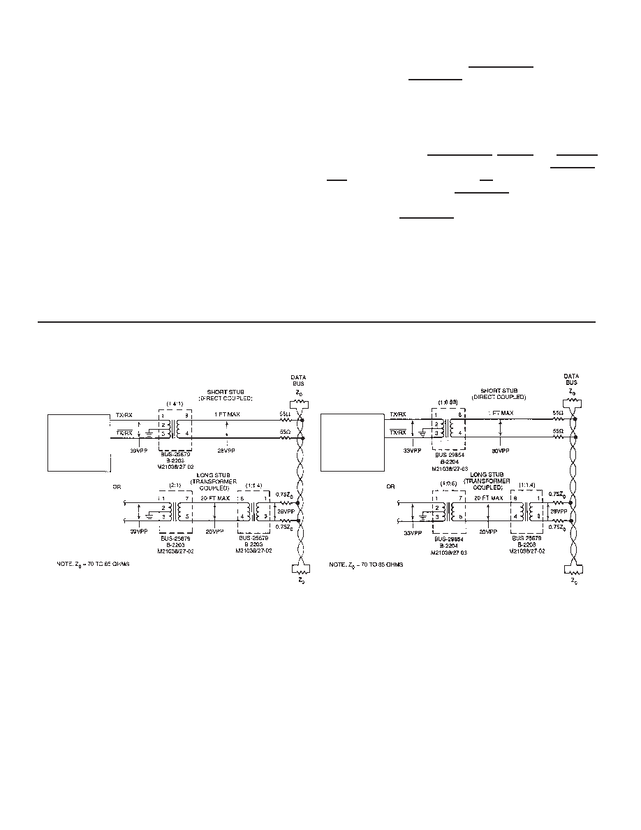
FIGURE 18. BU-61559X1, BU-61559X2 INTERFACE TO 1553 BUS
NOTES for FIGURE 18:
(1) Shown for one of two redundant buses that interface to the BU-61559/60 Series hybrid.
(2) Transmitted voltage level on 1553 bus is 6 Vp-p min, 7 Vp-p nominal, 9 Vp-p max.
(3) Required tolerance on isolation resistors is 2%. Instantaneous power dissipation (when transmitting) is approximately 0.5 W (typ), 0.8 W (max).
(4) Transformer pin numbering is correct for DDC BUS-25679 or BUS-29854 transformer. For the Beta transformer (e.g., B-2203) or the QPL-21038-31 transformer (e.g.,
M21038/27-02), the winding sense and turns ratio are mechanically the same, but the pin numbering is reversed. Therefore, it is necessary to reverse pins 8 and 4 or
pins 7 and 5 in the diagram for the Beta or QPL transformers.
In the buffered mode, the output MEMENA-OUT must be con-
nected to the input MEMENA-IN.
TRANSPARENT MODE
The transparent mode (reference FIGURE 20) supports an inter-
face to up to 64K words of external shared RAM and/or to a
STANAG-3910 component set. In the transparent mode, the
memory control signals MEMENA-OUT, MEMOE, and MEMWR
are used to read and write data from/to external RAM. MEMENA-
OUT is the BU-61559's Chip Select (CS) output signal. For inter-
nal RAM accesses, the input MEMENA-IN should be asserted
low. When there is no ongoing memory access, or for accesses
to external RAM, MEMENA-IN should be presented as a logic 1.
In the transparent mode, the address buffers drive the CPU
address onto the internal memory bus for CPU transfers; for
1553 transfers, the internal memory address is asserted on the
external address bus. The data buffers are directed outward for
BU-61559X1
BU-61559X2
相關(guān)PDF資料 |
PDF描述 |
|---|---|
| BU-61559F2-660Q | 2 CHANNEL(S), 1M bps, MIL-STD-1553 CONTROLLER, CDFP78 |
| BU-61559F2-810L | 2 CHANNEL(S), 1M bps, MIL-STD-1553 CONTROLLER, CDFP78 |
| BX80562X3230SLACS | 64-BIT, 266 MHz, MICROPROCESSOR, PBGA775 |
| BT457KG125 | PALETTE-DAC DSPL CTLR, CPGA68 |
| BU-61580D0-110 | 2 CHANNEL(S), 1M bps, MIL-STD-1553 CONTROLLER, CQIP70 |
相關(guān)代理商/技術(shù)參數(shù) |
參數(shù)描述 |
|---|---|
| BU-61580 | 制造商:未知廠家 制造商全稱:未知廠家 功能描述:MIL-STD-1553 Components |ACE |
| BU-61580G1-100 | 制造商:未知廠家 制造商全稱:未知廠家 功能描述:MIL-STD-1553/ARINC Bus Controller/RTU |
| BU-61580G1-110 | 制造商:未知廠家 制造商全稱:未知廠家 功能描述:MIL-STD-1553/ARINC Bus Controller/RTU |
| BU-61580G1-120 | 制造商:未知廠家 制造商全稱:未知廠家 功能描述:MIL-STD-1553/ARINC Bus Controller/RTU |
| BU-61580G1-200 | 制造商:未知廠家 制造商全稱:未知廠家 功能描述:MIL-STD-1553/ARINC Bus Controller/RTU |
發(fā)布緊急采購(gòu),3分鐘左右您將得到回復(fù)。