- 您現(xiàn)在的位置:買賣IC網(wǎng) > PDF目錄369517 > BT457KG125 Video DAC with Color Palette (RAMDAC) PDF資料下載
參數(shù)資料
| 型號(hào): | BT457KG125 |
| 英文描述: | Video DAC with Color Palette (RAMDAC) |
| 中文描述: | 視頻DAC的調(diào)色板(的RAMDAC) |
| 文件頁(yè)數(shù): | 16/60頁(yè) |
| 文件大小: | 647K |
| 代理商: | BT457KG125 |
第1頁(yè)第2頁(yè)第3頁(yè)第4頁(yè)第5頁(yè)第6頁(yè)第7頁(yè)第8頁(yè)第9頁(yè)第10頁(yè)第11頁(yè)第12頁(yè)第13頁(yè)第14頁(yè)第15頁(yè)當(dāng)前第16頁(yè)第17頁(yè)第18頁(yè)第19頁(yè)第20頁(yè)第21頁(yè)第22頁(yè)第23頁(yè)第24頁(yè)第25頁(yè)第26頁(yè)第27頁(yè)第28頁(yè)第29頁(yè)第30頁(yè)第31頁(yè)第32頁(yè)第33頁(yè)第34頁(yè)第35頁(yè)第36頁(yè)第37頁(yè)第38頁(yè)第39頁(yè)第40頁(yè)第41頁(yè)第42頁(yè)第43頁(yè)第44頁(yè)第45頁(yè)第46頁(yè)第47頁(yè)第48頁(yè)第49頁(yè)第50頁(yè)第51頁(yè)第52頁(yè)第53頁(yè)第54頁(yè)第55頁(yè)第56頁(yè)第57頁(yè)第58頁(yè)第59頁(yè)第60頁(yè)

1.0 Circuit Description
Bt457/Bt458
1.3 MPU Interface
125 MHz/135 MHz/165 MHz Monolithic CMOS 256 Color Palette RAMDAC
1-8
Conexant
L45801 Rev. N
Additional Information
Although the color palette RAM and overlay registers are dual-ported, if the pixel
and overlay data are addressing the same palette entry being written to by the
MPU during the write cycle, one or more of the pixels on the display screen can
be disturbed. A maximum of one pixel is disturbed if the write data from the
MPU is valid during the entire chip enable time.
The control registers are also accessed through the address register in
conjunction with the C0 and C1 inputs, as specified in
Table 1-3
. All control
registers can be written to or read by the MPU at any time. The address register
does not increment following read or write cycles to the control registers,
facilitating read-modify-write operations.
If an invalid address loads into the address register, data written to the device
is ignored, and invalid data is read by the MPU.
Frame Buffer Interface
To enable pixel data to be transferred from the frame buffer at TTL data rates, the
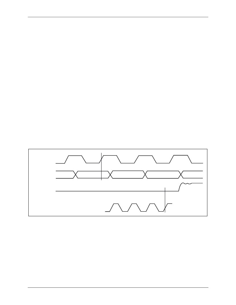
Bt457/458 incorporates internal latches and multiplexers. As illustrated in
Figure 1-3
, on the rising edge of LD*, sync and blank information, color (up to 8
bits per pixel), and overlay (up to 2 bits per pixel) information, for either 4 or 5
consecutive pixels, are latched into the device. With this configuration, the sync
and blank timing is recognized only with 4- or 5-pixel resolution. Typically, the
LD* signal is used to clock external circuitry to generate basic video timing.
Each clock cycle, the Bt457/458 outputs color information based on the {A}
inputs, followed by the {B} inputs, then the {C} inputs, etc., until all 4 or 5 pixels
have been output, at which point the cycle repeats.
The overlay inputs can have pixel timing, facilitating the use of additional bit
planes in the frame buffer to control overlay selection on a pixel basis. On the
other hand, they can be controlled by external character or cursor generation
logic.
To simplify the frame buffer interface timing, LD* can be phase shifted in any
amount relative to CLOCK. This enables the LD* signal to be derived by
externally dividing CLOCK by 4 or 5 independent of the propagation delays of
the LD* generation logic. As a result, the pixel and overlay data are latched on the
rising edge of LD*, independent of the clock phase.
Figure 1-3. Video Input/Output Timing
CLOCK
DATA
IOR, IOG, IOB
(IOUT
–
Bt457)
P[7:0] (A
–
E),
OL[1,0] (A
–
E),
SYNC*, BLANK*
LD*
457-8_014
相關(guān)PDF資料 |
PDF描述 |
|---|---|
| BT457KG80 | Video DAC with Color Palette (RAMDAC) |
| BT457KPJ110 | Video DAC with Color Palette (RAMDAC) |
| BT457KPJ125 | Video DAC with Color Palette (RAMDAC) |
| BT457KPJ80 | Video DAC with Color Palette (RAMDAC) |
| BT8472EPF | Protocol Controller |
相關(guān)代理商/技術(shù)參數(shù) |
參數(shù)描述 |
|---|---|
| BT457KG80 | 制造商:未知廠家 制造商全稱:未知廠家 功能描述:Video DAC with Color Palette (RAMDAC) |
| BT457KPJ110 | 制造商:BROOKTREE 功能描述: |
| BT457KPJ125 | 制造商:未知廠家 制造商全稱:未知廠家 功能描述:Video DAC with Color Palette (RAMDAC) |
| BT457KPJ135 | 制造商:BROOKTREE 功能描述: 制造商:Brooktree 功能描述:Digital Analog Converter, Single, 8 Bit, 84 Pin, PLCC 制造商:Brooktree (BT) 功能描述:Digital Analog Converter, Single, 8 Bit, 84 Pin, PLCC 制造商:BT 功能描述:Digital Analog Converter, Single, 8 Bit, 84 Pin, PLCC |
| BT457KPJ80 | 制造商:未知廠家 制造商全稱:未知廠家 功能描述:Video DAC with Color Palette (RAMDAC) |
發(fā)布緊急采購(gòu),3分鐘左右您將得到回復(fù)。