- 您現(xiàn)在的位置:買賣IC網(wǎng) > PDF目錄369509 > BT136-800F 8-Bit Multi-Level Pipeline Register 24-PDIP -40 to 85 PDF資料下載
參數(shù)資料
| 型號(hào): | BT136-800F |
| 英文描述: | 8-Bit Multi-Level Pipeline Register 24-PDIP -40 to 85 |
| 中文描述: | 晶閘管產(chǎn)品目錄 |
| 文件頁數(shù): | 186/224頁 |
| 文件大小: | 2697K |
| 代理商: | BT136-800F |

AN1009
Application Notes
http://www.teccor.com
+1 972-580-7777
AN1009 - 2
2002 Teccor Electronics
Thyristor Product Catalog
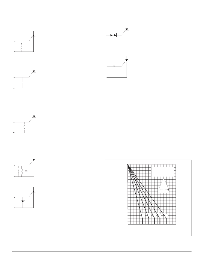
Examples of Gate Terminations
Primary Purpose
(1) Increase dv/dt capability
(2) Keep gate clamped to ensure V
DRM
capability
(3) Lower t
q
time
Related Effect
— Raises the device latching
and holding current
Primary Purpose
(1) Increase dv/dt capability
(2) Remove high frequency noise
Related Effects
(1) Increases delay time
(2) Increases turn-on interval
(3) Lowers gate signal rise time
(4) Lowers di/dt capability
(5) Increases t
q
time
Primary Purpose
(1) Decrease DC gate sensitivity
(2) Decrease t
q
time
Related Effects
(1) Negative gate current increases holding
current and causes gate area to drop out of
conduction
(2) In pulse gating gate signal tail may
cause device to drop out of conduction
Primary Purpose
— Select frequency
Related Effects
— Unless circuit is
“damped,” positive and negative gate current
may inhibit conduction or bring about spo-
radic anode current
Primary Purpose
(1) Supply reverse bias in off period
(2) Protect gate and gate supply for reverse
transients
(3) Lower t
q
time
Related Effects
— Isolates the gate if high
impedance signal source is used without
sustained diode current in the negative cycle
Primary Purpose
— Decrease threshold
sensitivity
Related Effects
(1) Affects gate signal rise time and di/dt
rating
(2) Isolates the gate
Primary Purpose
— Isolate gate circuit DC
component
Related Effects
— In narrow gate pulses
and low impedance sources, I
followed by
reverse gate signals which may inhibit con-
duction
Curves for Average Current at Various
Conduction Angles
SCR maximum average current curves for various conduction
angles can be established using the factors for maximum aver-
age current at conduction angle of:
30° = 0.40 x Avg 180°
60° = 0.56 x Avg 180°
90° = 0.70 x Avg 180°
120° = 0.84 x Avg 180°
The reason for different ratings is that the average current for
conduction angles less than 180° is derated because of the
higher RMS current connected with high peak currents.
Note that maximum allowable case temperature (T
) remains the
same for each conduction angle curve but is established from
average current rating at 180° conduction as given in the data
sheet for any particular device type. The maximum T
curve is
then derated down to the maximum junction (T
J
). The curves
illustrated in Figure AN1009.4 are derated to 125 °C since the
maximum T
J
for the non-sensitive SCR series is 125 °C.
Figure AN1009.4
Typical Curves for Average On-state Current at
Various Conduction Angles versus T
C
for a
SXX20L SCR
Zener
optional
80
85
90
95
100
105
110
115
120
125
0
2
4
6
8
10
12
14
16
Average On-state Current [I
T
(AV)] – Amps
M
C
)
C
10
9
3
6
10
Current: Halfwave Sinusoidal
Load: Resistive or Inductive
Conduction Angle: As Given Below
Case Temperature: Measured as
Shown on Dimensional Drawings
Conduction Angle
7.2
10.8
12.8
5.1
相關(guān)PDF資料 |
PDF描述 |
|---|---|
| BT136S | Triacs |
| BT136_SERIES | Transient Voltage Suppressor Diodes |
| BT136_SERIES_D | Transient Voltage Suppressor Diodes |
| BT136_SERIES_E | Transient Voltage Suppressor Diodes |
| BT136F700 | Transient Voltage Suppressor Diodes |
相關(guān)代理商/技術(shù)參數(shù) |
參數(shù)描述 |
|---|---|
| BT136-800G | 制造商:TECCOR 制造商全稱:TECCOR 功能描述:Thyristor Product Catalog |
| BT136B | 制造商:PHILIPS 制造商全稱:NXP Semiconductors 功能描述:Triacs sensitive gate |
| BT136B_SERIES_E | 制造商:未知廠家 制造商全稱:未知廠家 功能描述:Triacs sensitive gate |
| BT136B-500 | 制造商:PHILIPS 制造商全稱:NXP Semiconductors 功能描述:Triacs |
| BT136B-500D | 制造商:PHILIPS 制造商全稱:NXP Semiconductors 功能描述:Triacs logic level |
發(fā)布緊急采購,3分鐘左右您將得到回復(fù)。