- 您現(xiàn)在的位置:買(mǎi)賣(mài)IC網(wǎng) > PDF目錄362539 > AU5790D-T LAN Transceiver PDF資料下載
參數(shù)資料
| 型號(hào): | AU5790D-T |
| 英文描述: | LAN Transceiver |
| 中文描述: | 網(wǎng)絡(luò)收發(fā)器 |
| 文件頁(yè)數(shù): | 7/19頁(yè) |
| 文件大小: | 165K |
| 代理商: | AU5790D-T |
第1頁(yè)第2頁(yè)第3頁(yè)第4頁(yè)第5頁(yè)第6頁(yè)當(dāng)前第7頁(yè)第8頁(yè)第9頁(yè)第10頁(yè)第11頁(yè)第12頁(yè)第13頁(yè)第14頁(yè)第15頁(yè)第16頁(yè)第17頁(yè)第18頁(yè)第19頁(yè)
Philips Semiconductors
Preliminary specification
AU5790
Single wire CAN transceiver
7
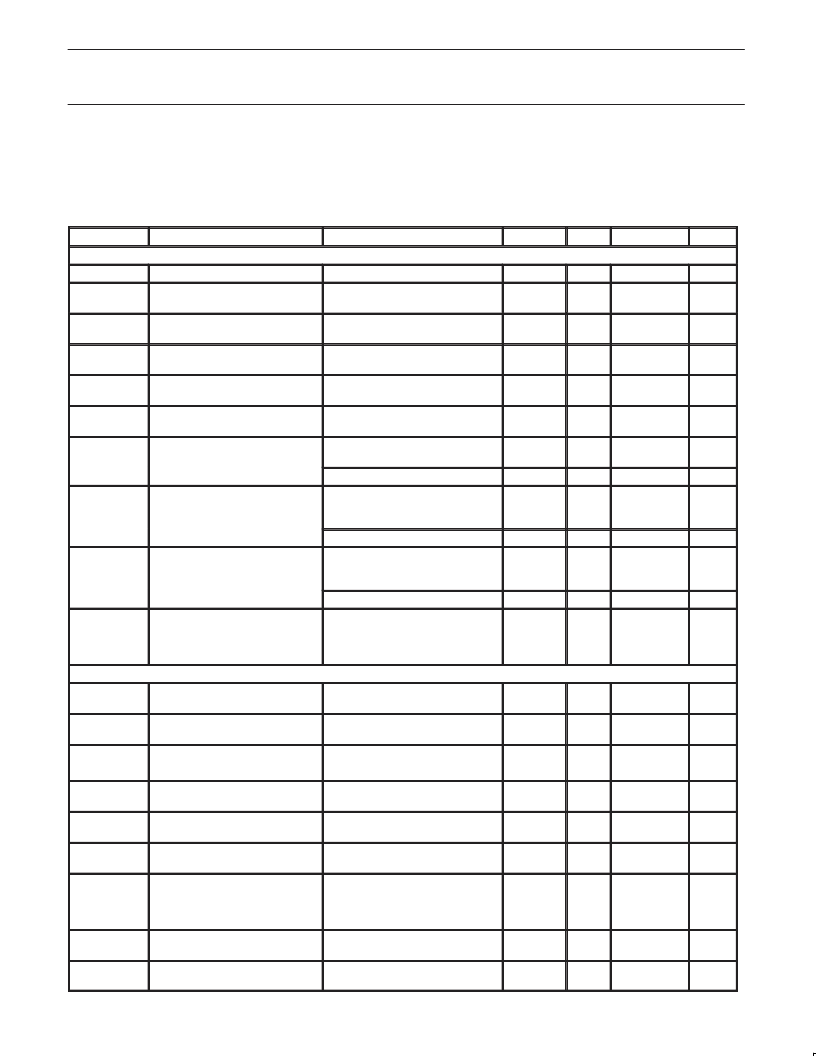
DC CHARACTERISTICS
–40
°
C < T
amb
< +125
°
C; 5.5 V < V
BAT
< 16 V; –0.3 V < V
TxD
< 5.5 V; –0.3 V < V
NSTB
< 5.5 V; –0.3 V < V
EN
< 5.5 V; –0.3 V < V
RxD
< 5.5 V;
–1 V < V
CANH
< +16 V; bus load resistor at pin RTH: 2 k
< R
T
< 9.2 k
; total bus load resistance
270
< R
L
< 9.2 k
;
C
L
< 13.7 nF; 1
μ
s < R
L
C
L
< 4
μ
s; RxD pull-up resistor 2.2 k
< R
d
< 3.0 k
; RxD: loaded with C
LR
< 30pF to GND;
all voltages are referenced to pin 8 (GND); positive currents flow into the IC;
typical values reflect the approximate average value at V
BAT
= 13 V and T
amb
= 25
°
C, unless otherwise specified.
SYMBOL
PARAMETER
CONDITIONS
MIN.
TYP.
MAX.
UNIT
Pin BAT
V
BAT
V
BATL
Operating supply voltage
Note 1
5.5
12
27
V
Low battery state
Part functional or in undervoltage
lockout state
2.5
5.5
V
V
BATLO
Supply undervoltage lockout state
TxD = 1 or 0; check CANH and
RxD are floating
2.5
V
I
BATPN
Passive state supply current in
normal mode
NSTB = 5 V, EN = 5 V, TxD = 5 V
2
mA
I
BATPW
Passive state supply current in
wake-up mode
NSTB = 0 V, EN = 5 V, TxD = 5 V,
Note 2
3
mA
I
BATPH
Passive state supply current in
high speed mode
NSTB = 5 V, EN = 0 V, TxD = 5 V,
Note 2
4
mA
I
BATN
Active state supply current in
normal mode
NSTB = 5 V, EN = 5 V, TxD = 0 V,
R
L
= 270
,
T
amb
= 125
°
C
T
amb
= –40
°
C
NSTB = 0 V, EN = 5 V, TxD = 0 V,
R
L
= 270
, Note 2,
T
amb
= 125
°
C
T
amb
= –40
°
C, Note 2
NSTB = 5 V, EN = 0 V, TxD = 0 V,
R
L
= 100
, Note 2,
T
amb
= 125
°
C
T
amb
= –40
°
C, Note 2
NSTB = 0 V, EN = 0 V, TxD = 5 V,
RxD = 5 V, –1 V < V
CANH
< +1 V,
5.5 V < V
BAT
< 14 V
–40
°
C < T
j
< 125
°
C
35
mA
40
mA
I
BATW
Active state supply current in
wake-up mode
70
mA
85
mA
I
BATH
Active state supply current in
high speed mode
70
mA
85
mA
I
BATS
Sleep mode supply current
70
100
μ
A
Pin CANH
V
CANHN
Bus output voltage in normal
mode
NSTB = 5 V, EN = 5 V,
R
L
> 270
; 5.5 V < V
BAT
< 27 V
NSTB = 0 V, EN = 5 V,
R
L
> 270
; 11.3 V < V
BAT
< 16 V
3.65
4.1
4.55
V
V
CANHW
Bus output voltage in wake-up
mode
9.80
min
(V
BAT
, 13)
V
V
CANHWL
Bus output voltage in wake-up
mode, low battery
NSTB = 0 V, EN = 5 V,
R
L
> 270
; 5.5 V < V
BAT
< 11.3 V
V
BAT
–
1.45
V
BAT
V
V
CANHH
Bus output voltage in high-speed
transmission mode
NSTB = 5 V, EN = 0 V,
R
L
> 100
; 8 V < V
BAT
< 16 V
Recessive state or sleep mode,
V
CANH
= –1 V; 0 V < V
BAT
< 27 V
Recessive state or sleep mode,
V
CANH
= 10 V; 0 V < V
BAT
< 16 V
TxD = 0 V, normal mode,
high-speed mode and sleep mode;
V
CANH
= 10 V;
0 V < V
BAT
< 16 V
V
CANH
= –1 V,
TxD = 0 V; NSTB = 5 V; EN = 5 V
3.65
4.55
V
I
CANHRR
Recessive state output current,
bus recessive
–10
10
μ
A
I
CANHRD
Recessive state output current,
bus dominant
–20
100
μ
A
I
CANHDD
Dominant state output current,
bus dominant
–20
100
μ
A
–I
CANH_N
Bus short circuit current,
normal mode
30
150
mA
–I
CANHW
Bus short circuit current,
wake-up mode
V
CANH
= –1 V,
TxD = 0 V; NSTB = 0 V; EN = 5 V
60
190
mA
Powered by ICminer.com Electronic-Library Service CopyRight 2003
相關(guān)PDF資料 |
PDF描述 |
|---|---|
| AUD02A48 | 10 Watts |
| AUD03F48 | 10 Watts |
| AUD03G48 | 10 Watts |
| AUD03M48 | 10 Watts |
| AUD03Y48 | 10 Watts |
相關(guān)代理商/技術(shù)參數(shù) |
參數(shù)描述 |
|---|---|
| AU5T-14474-CAA | 功能描述:汽車(chē)連接器 2.8MM FEM CBL SLD GRS RoHS:否 制造商:Amphenol SINE Systems 產(chǎn)品:Contacts 系列:ATP 位置數(shù)量: 型式:Female 安裝風(fēng)格: 端接類(lèi)型: 觸點(diǎn)電鍍:Nickel |
| AU610 | 制造商:MCM 功能描述:Connector |
| AU6254 | 制造商:未知廠家 制造商全稱(chēng):未知廠家 功能描述:USB2.0 Hub Controller |
| AU6320 | 制造商:未知廠家 制造商全稱(chēng):未知廠家 功能描述:USB2.0 CF Card Reader Controller |
| AU6331 | 制造商:未知廠家 制造商全稱(chēng):未知廠家 功能描述:USB2.0 SD/MMC/MS Single/Dual LUN Card Reader Controller |
發(fā)布緊急采購(gòu),3分鐘左右您將得到回復(fù)。