- 您現(xiàn)在的位置:買賣IC網(wǎng) > PDF目錄362539 > ATW2805S-MSTR Analog IC PDF資料下載
參數(shù)資料
| 型號: | ATW2805S-MSTR |
| 英文描述: | Analog IC |
| 中文描述: | 模擬IC |
| 文件頁數(shù): | 3/9頁 |
| 文件大小: | 113K |
| 代理商: | ATW2805S-MSTR |
3
ATW2812D
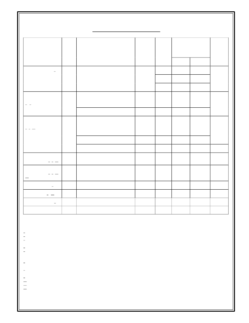
TABLE I. Electrical Performance Characteristics - Continued
Test
Symbol
Conditions
-55
°
C
≤
T
C
≤
+125
°
C
V
IN
= 28 V dc ±5%, C
L
= 0 unless
otherwise specified
Group A
Subgroups
Device
types
Limits
Unit
Min
Max
Switching frequency 4/
F
S
I
OUT
= 2500 mA
4,5,6
01
250
300
KHz
02
250
270
03
275
300
Output response to step
transient load changes
4/ 9/
VO
TLOA
D
1250 mA to/from 2500 mA
4,5,6
All
-400
+400
mV pk
0 mA to/from 2500 mA
4,5,6
All
-800
+800
Recovery time, step
transient load changes
4/ 9/ 10/
TT
LOAD
1250 mA to/from 2500 mA
4,5,6
All
70
μs
0 mA to/from 1250 mA
4,5,6
All
500
1250 mA to/from 0 mA
4,5,6
All
5
ms
Output response transient
step line changes 4/ 7/ 11/
VO
TLINE
Input step from/to 18 to 40 V dc,
I
OUT
= 2500 mA
4,5,6
All
-800
+800
mV pk
Recovery time transient
step line changes 4/ 7/ 10/
11/
TT
LINE
Input step from/to 18 to
40 V dc,
I
OUT
= 2500 mA
4,5,6
All
4000
μs
Turn on overshoot 4/
VTon
OS
I
OUT
= 0 and 2500 mA
4,5,6
All
750
mV pk
Turn on delay 4/ 12/
Ton
D
I
OUT
= 0 and 2500 mA
4,5,6
All
14
ms
Load fault recovery 7/
Tr
LF
4,5,6
All
14
ms
Weight
Flange
75
grams
Notes:
1/
2/
3/
4/
5/
6/
Parameter guaranteed by line load, and cross regulation tests.
Up to 90 percent of full power is available from either output provided the total output does not exceed 30 W.
Bandwidth guaranteed by design. Tested for 20 KHz to 2 MHz.
Load current split equally between +V
OUT
and -V
OUT
.
Three-watt load on output under test, 3 watt to 27 watt load change on other output.
Capacitive load may be any value from 0 to the maximum limit without compromising dc performance. A capacitive load in excess of the
maximum limit will not disturb loop stability but may interfere with the operation of the load fault detection circuitry, appearing as a short circuit during
turn-on.
Parameter shall be tested as part of design characterization and after design or process changes. Thereafter, parameters shall be guaranteed to the limits
specified in Table I.
8/
An overload is that condition with a load in excess of the rated load but less than that necessary to trigger the short circuit protection and is the condition
of maximum power dissipation.
9/
Load step transition time between 2 and 10 microseconds.
10/
Recovery time is measured from the initiation of the transient to where V
OUT
has returned to within ±1 percent of V
OUT
at 50 percent load.
11/
Input step transition time between 2 and 10 microseconds.
12/
Turn-on delay time measurement is for either a step application of power at the input or the removal of a ground signal from the inhibit pin (pin 8) while
power is applied to the input.
7/
相關PDF資料 |
PDF描述 |
|---|---|
| ATW2805S-SLV | Analog IC |
| ATW2815D-MSTR | Analog IC |
| ATW28XXD | ADVANCED ANALOG HYBRID-HIGH RELIABILITY DC/DC CONVERTERS |
| ATXP1 | Jumper Free Over Clock Controller |
| ATXP3 | Jumper Free Over Clock Controller |
相關代理商/技術參數(shù) |
參數(shù)描述 |
|---|---|
| ATW2805S-SLV | 制造商:International Rectifier 功能描述:DC/DC CONVERTER, FLANGED, MINIMUM SCREENING, SLAVE - Bulk |
| ATW2806S | 制造商:International Rectifier 功能描述:MODULE DC-DC 1-OUT 6V 6A 30W 10-PIN (10+TAB) ATW - Bulk |
| ATW2807D | 制造商:International Rectifier 功能描述:DC/DC CONVERTER, FLANGED, MINIMUM SCREENING - Bulk |
| ATW2812D | 制造商:International Rectifier 功能描述:DC/DC CONVERTER, FLANGED, MINIMUM SCREENING - Bulk |
| ATW2812D/CH | 制造商:International Rectifier 功能描述:DC/DC CONVERTER, FLANGED, CLASS H - Bulk |
發(fā)布緊急采購,3分鐘左右您將得到回復。