- 您現(xiàn)在的位置:買賣IC網 > PDF目錄378408 > ATR28XXS (International Rectifier) HYBRID-HIGH RELIABILITY DC/DC CONVERTERS PDF資料下載
參數資料
| 型號: | ATR28XXS |
| 廠商: | International Rectifier |
| 英文描述: | HYBRID-HIGH RELIABILITY DC/DC CONVERTERS |
| 中文描述: | 混雜高度可靠的DC / DC轉換器 |
| 文件頁數: | 6/12頁 |
| 文件大小: | 97K |
| 代理商: | ATR28XXS |
6
www.irf.com
ATR28XXS Series
Specifications
ABSOLUTE MAXIMUM RATINGS
Input Voltage -0.5V to 50V
Soldering Temperature 300
°
C for 10 seconds
Case Temperature Operating -55
°
C to +125
°
C
Storage -65
°
C to +135
°
C
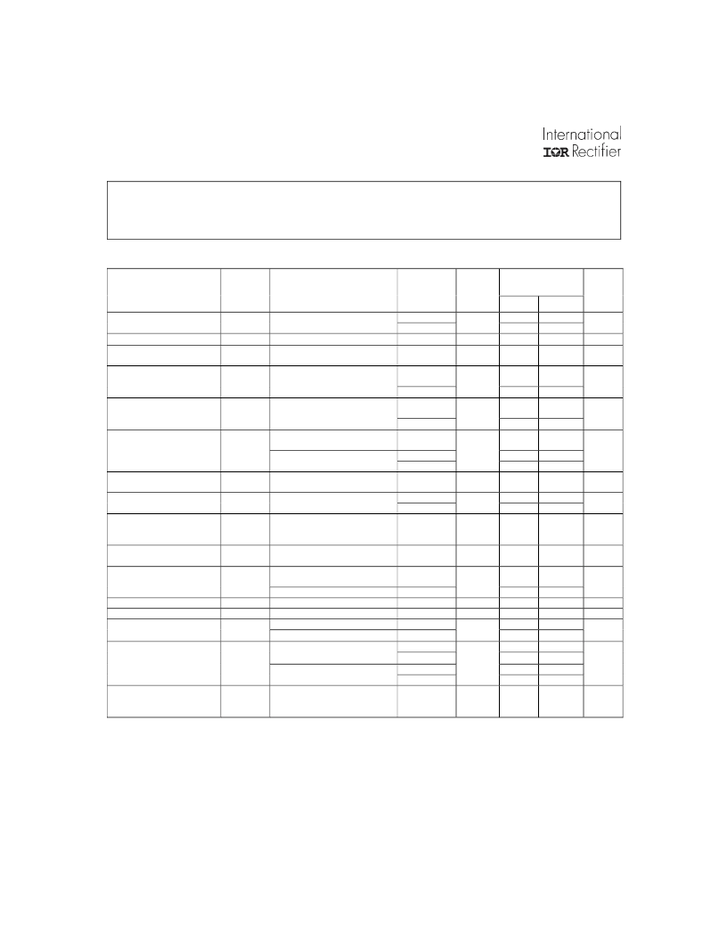
Table III. Electrical performance Characteristics
ATR2812S
Limits
Test
Symbol
Conditions
-55
°
C
≤
TC
≤
+125
°
C
V
= 28VDC
±
5%, C
= 0
Unless otherwise specified
I
OUT
= 0
V
IN
= 16, 28, and 40 VDC
V
= 16, 28, and 40 VDC
B.W. = 20Hz to 2 MHz
V
IN
= 16, 28, and 40 VDC
I
OUT
= 0, 1250, and 2500mA
V
IN
= 16,28, and 40 VDC
I
OUT
= 0, 1250, and 2500mA
I
= 0, inhibit (pin 2)
Tied to input return (pin 10)
I
OUT
= 0, inhibit (pin 2) = open
I
=2500mA
B.W. = 20Hz to 2 MHz
I
OUT
=2500mA
Input to output or any pin
To case (except pin 8) at
500 VDC, TC =+25
°
C
No effect on dc performance
TC =+25
°
C
Overload, TC = +25
°
C
Group A
Subgroups
Device
Types
Min
Max
Units
Output voltage
Output current
Output ripple voltage
V
OUT
I
OUT
V
RIP
1
2,3
1,2,3
1,2,3
01
01
01
11.88
11.70
12.12
12.30
2500
60
V
mA
mVp-p
1
2
Line regulation
3
VR
LINE
1
01
01
01
01
±
30
mV
mV
mA
mAp-p
Load regulation
2,3
1
±
60
±
60
3
VR
LOAD
Input current
2,3
1,2,3
±
120
18
I
IN
Input ripple current
1
2,3
1,2,3
50
75
50
2
I
RIP
Efficiency
Isolation
E
FF
I
SO
1
2,3
1
01
01
80
75
100
%
M
Capacitive load
4, 5
C
L
4
01
500
μ
F
Power dissipation
load fault
Switching frequency
Sync frequency range
Output response to step
transient load changes
Recovery time step
transient load changes
Output response to
transient step line
changes
P
D
6
1
01
01
01
01
01
01
12
W
KHz
KHz
mV pk
μ
s
mV pk
Short Circuit
I
OUT
= 2500mA
I
= 2500mA
1250mA to/from 2500mA
200mA to/from 1250mA
1250mA to/from 2500mA
200mA to/from 1250mA
Input step 16V to/from
40VDC, I
OUT
= 2500mA
1,2,3
4,5,6
4,5,6
4,5,6
4,5,6
4
5,6
4
5,6
4,5,6
9
F
S
F
SYNC
VO
TLOAD
TT
LOAD
VO
TLINE
500
500
-800
-1000
600
700
+800
+1000
100
200
100
200
±
1200
7
7, 8
For Notes to Specifications, refer to page 7
相關PDF資料 |
PDF描述 |
|---|---|
| ATTM01 | Processor Thermal Monitor |
| ATTM01G | Processor Thermal Monitor |
| ATTM01M | Processor Thermal Monitor |
| ATTM01MG | Processor Thermal Monitor |
| ATTM02 | Processor Thermal Monitor |
相關代理商/技術參數 |
參數描述 |
|---|---|
| ATR28XXS_07 | 制造商:IRF 制造商全稱:International Rectifier 功能描述:HYBRID-HIGH RELIABILITY DC/DC CONVERTER |
| ATR28XXT | 制造商:IRF 制造商全稱:International Rectifier 功能描述:HYBRID-HIGH RELIABILITY DC/DC CONVERTER |
| ATR30 | 制造商:Audio Technica 功能描述:Professional Microphone |
| ATR-30 | 功能描述:FUSE MICRO II BLADE 2 LEG 30 AMP 制造商:eaton 系列:* 零件狀態(tài):有效 標準包裝:5 |
| ATR3350 | 制造商:Audio Technica 功能描述:Lavalier Microphone |
發(fā)布緊急采購,3分鐘左右您將得到回復。